October 19th news, according to Nikkei news report, Samsung Electronics held a wafer foundry business briefing in Tokyo, Japan on the 18th to show customers the technology and production capacity outlook, with the goal of further expanding its wafer foundry business in Japan.
It is worth noting that Kumamoto wafer factory (JASM), jointly invested and operated by TSMC, Sony Semiconductor Solutions and Nippon Densco, started construction in Japan in April this year, with a total investment of US$8.6 billion. It aims to start mass production of 22-28nm processes by the end of 2024, with a monthly production capacity of 55,000 12-inch wafers. In the future, it will also be upgraded to a higher performance 12~16nm process, and it will not be ruled out that the process will be improved in the future.
To a certain extent, TSMC's layout in Japan seems to stimulate , Samsung , further increasing its attention to the Japanese wafer foundry market.
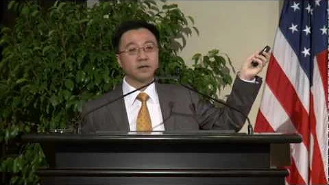
Samsung's wafer foundry department deputy president said, "Although the business scale of the Japanese market is not as large as that of the United States and other markets, it is growing rapidly and expanding, which is a very important market. The Japanese market is expanding rapidly in the fields of automobiles, consumer electronics, IoT, etc., and we will further seize the market." The vice president of
pointed out that Samsung's wafer foundry customers have increased by more than twice since 2019 and are expected to grow to five times by 2027.
In addition, Cui Shirong, the president of Samsung in charge of wafer foundry business, also reiterated at the briefing that Samsung "plans to start mass production of 2nm process technology in 2025 and 1.4nm in 2027."
report pointed out that Samsung is actively investing in its wafer foundry business, and the equipment investment will increase to 10 times within 8 years, and plans to increase the advanced process capacity to three times the current level by 2027, and the mature process capacity will also increase to 2.5 times the current level.
Yesterday, Samsung Electronics also announced that it plans to expand its multi-project wafer (MPW) service in 2023, and its process technology will be expanded to 4nm. The so-called multi-project wafer refers to the chip service where multiple integrated circuit designs using the same process are placed on the same wafer. After the manufacturing is completed, dozens of chip samples can be obtained for each design. It can help chip design companies reduce the cost of chip cutting.
reported that as the risk of geopolitical rises, the procurement strategies of wafer foundry customers have also changed. According to Samsung's Japanese subsidiary, "there are more inquiries from Japanese customers about BCP (Operation Continuing Plan) than before."
Edit: Xinzhixun-Linzi