Samsung GAA 3nm mass production has entered the countdown.
Volume production of three-nanometer engineering may be announced within this week.
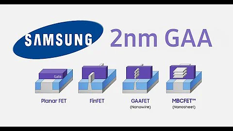
reduces the size and improves power efficiency.

Samsung Electronics has entered the countdown to mass production of 3nm engineering based on the new generation Gate-All-Around for the first time in the world. The GAA new project is evaluated as the "winner" for Samsung Electronics to catch up with Taiwan's TSMC, which ranks first in the world's chip (semiconductor contract production). This is the 3nm project mass production that started about 6 months before TSMC, seizing Qualcomm , Nvidia and other core customers, and even getting rid of the pursuit of Intel which announced its re-entry into English .
" Samsung management is very determined to mass produce three nanometers"
According to the semiconductor industry on the 28th, Samsung Electronics is expected to officially announce the mass production of its GAA-based 3 nanometer project within this week. It is reported that Samsung Electronics is internally discussing whether to also announce relevant content to secure new customer companies based on 3 nanometers.
Although there are rumors that Samsung Electronics has failed to overcome technical limitations and will delay mass production, company officials flatly rejected this rumor. An industry source said: "As far as I know, the development of 3-nanometer GAA semiconductors is proceeding smoothly according to the existing plan. Since the management has a very strong will to mass-produce 3-nanometer within the first half of the year, there may be plans this week. News. "Through this mass production, Samsung Electronics is expected to take the lead in ultra-fine and fair competition among world semiconductor companies. Because 3 nanometers is equivalent to reducing the width of a semiconductor circuit to 3/100,000 of the thickness of a human hair. The finer the circuit spacing of semiconductor , the higher the performance and the less power consumption. As the number of semiconductors produced from wafers (semiconductor masters) increases, production efficiency will also improve. This is why the semiconductor industry is competing in nanotechnology.
Samsung Electronics has added a new GAA project on this basis. In other words, the manufacturing technology of transistors that switches for the flow of current within the semiconductor is simply changed. FinFET technology, named after its shape like a shark fin, is currently used in semiconductor engineering. However, as the size of semiconductors continues to shrink, it has encountered limitations in current control. This is because the gate, which controls the current, fails to function as it should and generates leakage current, resulting in a decrease in power efficiency.
On the contrary, the GAA structure can adjust the flow of current more finely, so the power efficiency will be further improved. The pin-pet has 3 current channels, but the structure of GAA is such that current passes through all sides, so the size of the transistor will become smaller. Therefore, semiconductors can ultimately be miniaturized. If the 3nm GAA project is used, compared with 7nm finpet, the chip area can be reduced by 45% and power consumption can be reduced by 50%. Performance is also expected to improve by around 35%. This technology is highly compatible with finpet engineering and has the advantage of being able to use existing equipment and technology intact.
The key is to ensure a stable yield
The industry believes that a stable yield (good product ratio) and ensuring customer companies are the key. Because of recent rumors that the profitability of Samsung Electronics' 3-nanometer semiconductors has declined, people have expressed doubts about the possibility of Samsung Electronics' successful mass production. In the 3nm mass production process, the more semiconductors per wafer survive, the higher the profits will be, which can reduce semiconductor prices. This is the biggest reason why customer companies choose semiconductor companies.
Samsung Electronics' technological capabilities are coming faster than expected. According to observations, Samsung Electronics' "System Semiconductor Outlook 2030", which aims to become the number one in the system semiconductor field by 2030, will also be on the right track starting from the disclosure of 3 nanometers.
TSMC has also stated that it plans to mass produce 3-nanometer semiconductors in the second half of this year.