Recently, Academician of the Chinese Academy of Engineering Ni Guangnan wrote an article pointing out that China's self-developed chips should make good use of the open source model and focus on the RISC-V architecture. What is the development trend of the RISC-V architecture at home and abroad? Why is it said that open source chips are an important opportunity for China?
Recently, Ni Guangnan, an academician of the Chinese Academy of Engineering, wrote an article in the "Digital World Special Issue", pointing out that my country's chip industry has always been subject to the "mainstream CPU" architecture, and there is still a big gap between the overall ecology and the international advanced level.
At present, X86 architecture and ARM architecture constitute the two mainstream camps of logic digital chips at present, forming a de facto chip "block" which makes us strongly depend on it. Although Intel now has opened up X86 architecture authorization, the initiative is completely in the hands of others. The same is true for ARM architecture, and it can stop authorization at any time, but now, we are ushering in a new opportunity.
This opportunity is an open instruction set architecture that has shown strong development potential. It is the RISC-V instruction set architecture. The RISC-V streamlined instruction set adopts an open source model, its architecture is advanced, easy to customize, and the ecosystem is still in its early stages of development. In other words, we can completely form our own controllable chip instruction set architecture, which provides development opportunities for my country's intelligent connection era to grasp the initiative in the development of the chip industry.
Therefore, Ni Guangnan suggests that we should actively seize the opportunities of the times, plan the development of my country's chip industry from a global perspective, focus on the open source RISC-V architecture, and promote the arrival of a new pattern of the world's chip industry.
At the beginning of this year, the "Xiangshan" open source high-performance RISC-V processor chip was successfully operated, marking the gradual implementation of an open source main line in the field of open source CPUs. It has the hope that it will be widely used by the industry and support the academic community to experiment and innovative ideas. What are the advantages of RISC-V chip architecture? Why is it said that open source chips are an important opportunity for China? What is the relationship between the "14th Five-Year Plan" and the "innovation alliance" model vigorously advocated in the Outline of the 2035 Vision Goals and the open source chip ecosystem?
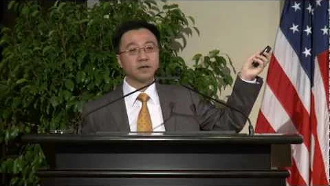
On March 19, the Capital Science Lecture Hall invited Deputy Director and Researcher Bao Yungang from the Institute of Computing Technology, Chinese Academy of Sciences, to tell the story of the development history and new trends of processor chips, as well as the story of Chinese scientists opening up new directions for open source chips.
The following is the speech video and the full text transcript:

The guest speaker:
Baoyungang
Deputy Director and Researcher of the Institute of Computing Technology, Chinese Academy of Sciences
◈ ◈ ◈ ◈
What is a chip
People often see chips in their lives. When we open the circuit board , many small black squares on the circuit board are common chips.
If you open these chips again and enlarge them hundreds of times, we will find that in fact, the chip design is very similar to urban planning. The inside of the chip is like a small city, with houses (some modules inside the chip), roads (connections between chip modules)... On a chip the size of a fingernail, there are hundreds of millions or even billions of small components, and they all have to be connected, so it is very complicated.
The most complex type of chip is processor chip. We call it the "jewel in the crown" of the chip industry. This type of chip design is very complex and difficult. Typical processor chips include a central processing unit (hereinafter referred to as CPU). The Loongson CPU developed by our country belongs to this type of central processing unit chip.
The artificial intelligence chip that people often see in recent years is also called a deep learning processor, which is also a type of processor chip. When playing games, we see gorgeous graphics and cool animation effects, behind which is the graphics processing unit (GPU for short).
processor chip is called the "brain" of electronic devices, and processor chips are indispensable in almost all electronic devices. At the same time, it is also a country's strategic industry. According to statistics, the scale of my country's information industry exceeded 16 trillion in 2018, accounting for 1/6 of the national GDP. Among them, processor chips, as the "cornerstone", support a total of more than 10 trillion electronic equipment manufacturing industries.
Let’s review the “past and present” of the chip. The processor chip is actually closely connected to the first computers in the early days. The world's first electronic computer, ENIACh, was invented in 1946. Behind it is actually an enlarged version of the processor. This processor uses a light bulb for computing. Why do electronic computers use light bulbs to make the most basic components? It is very important that the light bulb can be used to indicate on and off. When power is on, the light bulb is on, which means "on"; when power is off, the light bulb is off, which means "off". This light bulb is also called tube . In this way, "on" and "off" can be mathematically easy to connect with "1" and "0".
705, German mathematician Leibniz discovered that 0 and 1 can also represent various numbers. For example, if the decimal number 7 is represented by 0 and 1, it can be represented as "1 1 1"; if the decimal number 6 is represented by 0 and 1, it can become "1 1 0". And binary numbers can also be used for operations. The invention of the binary computing system laid the foundation for today's computer computing.
But the bulb is still too large. Like the first electronic computer, ENIAC, there are a total of more than 18,000 tubes of light bulbs. So many electronic tubes combined make it weigh 30 tons and cover an area of about 170 square meters. It requires a large house to be placed. How can I make this switch smaller?
947, three scientists, Badin , Bratton and Shockley, discovered a material called semiconductor that can be used as switches, so they invented the transistor based on semiconductor material . They won the 1956 Nobel Prize in Physics . In 1957, engineer Kilby connected the transistors and circuit components together and placed them on a semiconductor base plate. This is the world's first integrated circuit, and he also won the 2000 Nobel Prize in Physics.
As the transistor volume further shrinks, the volume of the integrated circuit continues to shrink. Today we use light on an semiconductor base plate about 1 square centimeter about the size of a fingernail, and can carve billions of transistors. This is a modern chip. Therefore, chips are actually a super-large-scale integrated circuit.
integrated circuit is our country's largest imported product. In 2020, my country imported about 500 billion integrated circuits, with an import value of up to US$350 billion, far exceeding the second-ranked oil of more than US$170 billion. Of the $350 billion integrated circuit chips, processor chip imports exceed US$170 billion, accounting for 49%. From a global perspective, the proportion of processor chips produced in China is actually less than 5%. So this is why we say that processor chips are my country's core strategic industry. We need more efforts to develop, grow and strengthen domestic chips, especially processor chips.
◈ ◈ ◈ ◈
processor chip is developed
When we want to make a processor chip, first, we need to have an instruction set . Instruction sets are actually a standard and a specification. For example, the size of screws and nuts is a standard specification. If the diameter of the screws and nuts is agreed, the inner diameter and outer diameter are 5 mm. Following this standard, products produced by different manufacturers can be screwed together. In fact, the instruction set also has the same function, except that it is a standard and specification formed between software and hardware. Follow the same instruction set to develop software and manufacture hardware. Software and hardware produced by different manufacturers can work together. This is the role of the instruction set.Each instruction in the
instruction set has its own functions, such as addition instructions, subtraction instructions, multiplication instructions, comparison instructions, etc. When we combine thousands of such instructions, we form an instruction set manual. Developing a processor through this manual is like giving you a dictionary to write a novel.
The entire chip production process includes design, manufacturing and packaging testing. First of all, design. After getting a manual for instruction set, we need to design it microarchitecture and describe how to implement it internally by completing up to hundreds of documents. After having the design document, developers need to describe the document in code and carry out engineering development. With the code, we also need EDA's tools, namely the electronic design automation tool - which can automatically translate this code into the layout inside the chip. The layout is about designing how to place hundreds of millions of transistors. Next is manufacturing and packaging testing. According to the territory, manufacturers can manufacture wafer and then hand it over to the packaging and testing companies, becoming such a chip we often see.
The entire manufacturing process is a bit like when we hand over the written novel to the publisher and print it out. However, in the chip field, this process is equivalent to printing the novel content on silicon wafer , and the steps are very complicated. Therefore, cutting-edge equipment like the lithography machine is needed, which is also an aspect that my country urgently needs to step up its improvement.
◈ ◈ ◈ ◈
Open source: New trend in the development of processor chips
Next, I will introduce to you the new trend in the development of processor chips - open source. What exactly is an open source chip?
In the entire chip design stage, that is, from an instruction set manual to the formation of the layout, it actually includes three levels: open source, design documents, and process tools, and open source for the whole world. Open source chips are just starting, but around the world, many people are already working in this direction. I believe that in the next 5-10 years, we will see some very big progress.
Our country also attaches great importance to open source and has made relevant layouts. The 14th Five-Year Plan clearly mentioned: it is necessary to support the development of innovation consortiums such as digital technology , open source community , improve open source intellectual property rights, and legal system, and encourage enterprises to open software source code, hardware design and application services.
In fact, not only my country is paying attention to it, but everyone around the world is paying attention to open source chips. In October 2019, The Economist wrote an article predicting: "Open source software is a prerequisite for the great development of smartphones in the past decade. And open source hardware like RISC-V may allow other devices to achieve similar expansion in the next decade." Why did
form such a trend? There are actually three driving forces behind it. The first is the fragmented demand of the intelligent Internet of Things (AIoT). The rise of the smart Internet of Things represents the arrival of the era of Internet of Things. Many items can be connected to the network and embedded into chips, becoming more and more intelligent. For example, the cup embedded in the chip can sense the passing person and show the smiling face. Today's chip demand is at the scale of 10 billion, and in the future, chip demand may be above 100 billion, so the chip demand is at least an order of magnitude greater than now. The problem behind the demand increment of
is fragmentation. Cup chips and curtain chips are obviously different, while Intel and ARM companies' traditional chip production methods are no longer able to cope with massive fragmented demands. Because if they want to do it, it often requires thousands of people to invest to make a chip. Therefore, we need to have new ways to solve the chip needs in the era of smart Internet of Things.
We can learn from open source software. Because open source software has lowered the threshold for APP development, three or five people can build an APP, which has brought the advantages of the Chinese population and has also attracted more talents and funds in my country's Internet industry, thus becoming competitive internationally.This is an effective way for open source software to lower the threshold to deal with fragmented needs, and this is a good example.
The second driving force is the desire for chip talents. The "bottleneck" dilemma is ultimately a lack of sufficient talents. Especially in the field of processor chips, there is a shortage of design talents. How to better solve the problem of talent shortage is an important breakthrough for us to deal with the dilemma of chip "bottleneck".
Reducing the threshold for chip design is an effective means. In the 1970s and early 1980s, the United States also encountered the problem of insufficient talent reserves. A 1982 statistics show that less than 100 professors and students from thousands of universities across the United States are engaged in chip and semiconductor related research. How did the United States solve it?
981, the United States launched the MOSIS project to provide universities with streaming and other services, with the purpose of lowering the design threshold of chips so that students can also make chips. In the past 40 years, this project has shipped more than 60,000 chips to American universities and research institutions and trained tens of thousands of students. In fact, it has effectively solved the problem of lack of chip talents.
The third driving force is from an industry perspective. lowering the threshold for chip design can actually help us better promote industrial changes, or have the opportunity to nurture some new industries. The MOSIS project mentioned above proposed a model called MPW (Multiple Project Wafer) model, which reduces chip design costs in order of magnitude. More importantly, this model separates manufacturing and design. In other words, some companies do not need to build manufacturing factories. They only need to focus on design to survive and develop well.
MOSIS project not only cultivated tens of thousands of students, but more importantly, it also gave birth to a new business model in the semiconductor field, which is what we call "fabless". The Fabless model has made the entire semiconductor industry more subdivided, allowing some companies to focus more on design, while others focus on OEM and manufacturing. This model has nurtured companies like AMD, Qualcomm , and Nvidia. In fact, they are all fable companies, all focusing on design. There are also companies focusing on OEM, such as TSMC and SMIC . Therefore, lowering the threshold for chip design will help prosper the entire market and industry.
◈ ◈ ◈ ◈
RISC-V development trend at home and abroad
We hope to lower the threshold for chip design within ten years, so that there will be no difficult chips in the world in the future. Undergraduates can also make chips and graduate with their own designed chips. Let a team of three or five people dare to start a chip startup company, making making chips as simple as writing an APP. To achieve this vision, we need to build an open source chip ecosystem. This ecological goal is to ultimately achieve that users only need to do 10% of their own chip design code.
How to build an open source chip ecosystem? The first is to have an open and free instruction set, which is the basis of the open source chip ecosystem. For more than half a century, almost all the instruction sets of processor chips belong to the company.
In 2010, several professors at the University of California, Berkeley proposed a new slogan: Instructions should be free. They created the prototype of the open source RISC-V instruction set. When the instruction set is open and free, a new way of building a processor chip ecosystem can be brought about. This ecological construction method is an open, open source, shared and co-governance model. After the standards are formulated, a manual for instruction set is formed, and enterprises around the world develop their own products based on the standards of this manual. Under this model, whoever invests more and makes greater contributions will have greater dominance. In recent years, China's contribution to the RISC-V ecosystem is becoming increasingly important.
RISC-V International Foundation was established in 2015 and is headquartered in Swiss . It is responsible for coordinating everyone to formulate standards for instruction sets. The Institute of Computing Technology of the Chinese Academy of Sciences is also a founding member. The foundation currently has more than 2,300 members from more than 70 countries around the world.
In 2018, China Open Directive Ecological Alliance, China RISC-V Industry Alliance, etc. were established in China one after another. These alliances have organized hundreds of Chinese companies, universities, and some research institutions to jointly promote the development of the RISC-V ecosystem.
At present, RISC-V is showing a booming trend throughout China and the whole world. Some institutions predict that by 2025, the world's RISC-V chips will exceed 60 billion. Another prediction is that RISC-V will also have a place in the data center field in 2030. Therefore, the ecological prospects of RISC-V are promising in the future.
◈ ◈ ◈ ◈
Open Source Chip Practice: "Xiangshan" and "One Life One Chip"
Next, I would like to talk to you about our related practices in the field of open source chips.
We have recently developed an open source high-performance RISC-V processor core with internationally advanced performance called "Xiangshan". We hope that it can become an open source main line like the Linux operating system, which can be widely used by the industry and allow the academic community to experiment with innovative ideas. More importantly, we also hope that "Xiangshan" can live for at least 30 years like Linux. At present, the "Xiangshan" chip has also been successfully cut, and it can run various software.
"Xiangshan" micro-architecture design, we use lakes to represent it. The microstructure of the first generation of "Xiangshan" is called Yanqi Lake, which is located in Huairou, Beijing. This is also because many of the students who participated in "Xiangshan" are undergraduates and graduate students from University of Chinese Academy of Sciences. They spend a year in Yanqi Lake when they were in the first grade, so they have a lot of feelings for Yanqi Lake, so they use the name Yanqi Lake. This chip has now been successfully cut, can work normally, and has achieved the results we expected.
The second generation of "Xiangshan" is called Nanhu, which was officially launched in May 2021. This name is also a tribute to the 100th anniversary of the founding of the Party. The architectural performance of Nanhu is greatly improved compared with the architectural performance of Yanqi Lake, with a frequency of 2G Hz, and its expected peak will be 1 times higher than the entire Yanqi Lake architecture.
is actually not just open source code in the open source chip field, but more importantly, it is to open up the process. So we have developed a lot of infrastructure, and these chip development infrastructure will be opened for the entire community to use together. We often use "iceberg" to describe the "Xiangshan" project - in fact, the chips you see are just the part that floats on the water. More importantly, the chip development infrastructure below the water surface, and we spend a lot of work on infrastructure research and development.
The "Xiangshan" project has received positive reviews at home and abroad. Some experts from abroad believe that the "Xiangshan" project has shown some of the power of the open source instruction set, and some experts even hope to participate in similar projects during college. They believe that it is very admirable that this project has been completed by a university team. This is also a contribution to the world by our open source project initiated by China as a Chinese team.
Next step, we are also exploring some new modes, the so-called "N+1" mode. That is, through similar open source projects, we will work with multiple companies to develop a chip. Because the model is open source, that is, the development process is open, every enterprise can participate at any time and its contribution can be recognized.
The second practice we want to share with you the plan for the cultivation of chip talents, that is, the "one life, one chip" plan. Its goal is to hope that undergraduates can also graduate with their own designed processor chips.
In August 2019, this project was officially launched at the University of Chinese Academy of Sciences. It is also the first time in China that it aims to drill the chip as its goal, guiding 5 undergraduate students to complete a RISC-V chip design within 4 months and successfully drill the chip. This chip is a SMIC 110-nanometer process that can run to a frequency of 200 megabyte-350 megabyte. It successfully runs the Linux system, and the students named it "Fruit Keel".Although the chip
is an undergraduate teaching chip, it also supports the undergraduate graduation design of these five students, one of them also obtained the Beijing Excellent Graduation Thesis. Finally, by participating in the "One Life One Chip" project, these five students achieved the goal of graduation with their own designed processor chips, and completed the journey from "super hardcore admission notice " to "super hardcore graduation certificate".
"One Life One Core" plan has been implemented for three periods, from 5 students in the first period to 11 students in the second period, and until about 100 students in the third period. In fact, in the third phase, there were 168 universities from home and abroad, and more than 760 students signed up. These students participated in the training process of the "One Life One Chip" plan. Although not all students have completed chip streaming, we are still further improving the "One Life One Chip" plan - by combining open source with chip design and talent training, more and more students finally make chips.
Through hard work, we are gradually lowering the threshold for chip design. Looking back on 2018, we formulated a "three-step" plan: the first step is to hope that through 3-5 years, the entire industry can obtain open source processor cores - "Xiangshan" is actually a very important output in this plan. The second step of
was to be able to use the open source EDA tool chain to make open source chips. This took 5-7 years, and we are still working hard on this step. We also envision undergraduates using these open source tools to complete the design of an open source chip and finally graduate with the designed chip. Unfortunately, we have not done it yet, but at least we have completed half of it through the "One Life One Core" plan, and we will work hard to do it in this direction next. Ultimately, we hope that by around 2030, chips can be designed automatically and intelligently through open source tool chains.
(Source: "Capital Science Lecture Hall" WeChat public account No. 738, ZAKER information)
Produced by: Science Popularization Central Kitchen
Produced by: Beijing Science and Technology News | Beike Media