Changdian Technology stated on the interactive platform that the company can realize the packaging and testing of 4nm mobile phone chip , as well as the integrated packaging and testing of CPU, GPU and radio frequency chips.
breaks the blockade! Changdian realizes 4nm mobile phone chip packaging
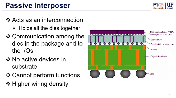
Changdian said that compared with traditional chip stacking technology, the advantage of multi-dimensional heterogeneous packaging and testing is that it can achieve higher density chip packaging and testing by introducing interposers and its multi-dimensional combination. At the same time, Multi-dimensional heterogeneous packaging and testing can achieve an effective balance between performance and cost by optimizing the combination of different densities of wiring and interconnection through the interposer.
html On June 13, Changdian Technology also stated that the company has been cooperating with different wafer factories on the silicon nodes of advanced processes and carried out related technology research and development and project development with major customers in the industry. It now has 5 and 7nm. The mass production capabilities of the wafer process enable customers to complete the mass production of high-performance computing chips and smart terminal main chip products.
In the field of semiconductor packaging and testing, Changdian Technology is the first in China and the third in the world. Its market share is second only to Sun Moonlight and Amkor.
Changdian Technology In the first quarter of 2022, the company achieved operating income of 8.14 billion yuan, a year-on-year increase of 21.2%; it achieved a net profit attributable to shareholders of listed companies of 860 million yuan, a year-on-year increase of 123%. First-quarter revenue and net profit both hit record highs for the same period in history.
Changdian Technology stated that the profit growth in the first quarter was mainly due to the company's continued focus on high-growth, high value-added products, actively optimizing customer and product structure, and improving profitability. At the same time, the company continues to take measures to reduce costs and increase efficiency, partially overcoming the pressure brought by rising material costs, power costs, transportation costs, etc., and maintaining continued improvement in profitability.
Over the years, as the development trend of chips has become more and more integrated and miniaturized, previous packaging and testing technologies have been unable to effectively seal and test lower nanometer chips to ensure product yield. Therefore, packaging and testing play an increasingly important role in the industry chain, and many domestic companies are also making efforts.
Speaking of closed testing, it is difficult not to mention Tongfu Microelectronics .
Tongfu Microelectronics strides forward
At the end of last year, Tongfu Microelectronics, as the fifth largest chip packaging and testing manufacturer in the world and the second largest in China, broke through the key technologies of high-density and high-reliability electronic packaging and testing and complete sets of processes, and won the national First Prize for Scientific and Technological Progress. This breakthrough chip packaging and testing technology is to solve the problems of easy bridging of solder joints and easy damage of interfaces in the high-density chip packaging and testing process. Flip-chip copper pillar bump high-density bonding technology is proposed. , this technology breaks through the bottleneck of high-density and reliable electronic packaging and testing technology, and solves the technical problems of electronic packaging and testing technology from 14 nanometers to 7 nanometers.
Recently, Tongfu Microelectronics stated that the company has mass-produced Chiplet products and 7nm products. Large-scale mass production has been completed, and 5nm products have completed research and development and are about to be mass-produced. The technical strength has risen to an unprecedented level. The company's advanced packaging and testing revenue has exceeded 70%. With the continuous development of packaging and testing companies in mainland China, Tongfu Microelectronics. It is also making great strides.
Currently, packaging and testing is a dynamic market, and a variety of packaging and testing technologies are booming. In terms of packaging and testing, Chinese companies have made great progress in
packaging and testing. Zhongzhanjiu

Judging from the ranking of the Top 10, only Ankou is an American company, and the others are all Chinese companies (including Taiwan Province of China).
Among these 9 companies, 3 are mainland Chinese companies, namely Pai. Jiangsu Changdian, Tongfu Microelectronics, and Tianshui Huatian ranked 3rd, 6th, and 7th. There are also 6 companies from Taiwan, ranking 1st, 4th, 5th, 8th, 9th, and 10th.
is well known. Among the design, manufacturing, packaging and testing of the entire semiconductor industry chain, the packaging and testing industry is the field with the highest technological maturity and the earliest breakthrough in the domestic semiconductor industry chain. In the past six months, the semiconductor industry has been severely out of stock, with upstream wafers. There is an urgent shortage of production capacity in OEMs and IDM factories. Global packaging and testing companies have successively increased their capital expenditure levels and expanded factories and equipment to cope with the growing demand. Mainland packaging and testing manufacturers are still handing over products one after another in the face of such a tight supply and demand environment. Brilliant report card.
These nine Chinese companies have taken a total of about 81% of the market share. They can be said to have truly monopolized the market share and have real control. Mainland Chinese companies also accounted for about 27% of the total, more than a quarter of the world's share.
From the perspective of growth rate, the three major enterprises in mainland China performed very well this time. Jiangsu Changdian grew by 27.5%, while Tongfu WeChat and Tianshui Huatian grew by 59.8% and 57.6% respectively, which were the highest growth among the Top 10. Two companies soon. In addition, my country's top ten integrated circuit packaging and testing companies are mainly concentrated in the Yangtze River Delta region, of which four are from Jiangsu. It is worth noting that emerging companies in some subdivisions, such as Suzhou Jingfang, are also leveraging their strengths and constantly moving to the forefront, and will become rising stars in the industry.
Opportunities for the development of China's packaging and testing industry
Policy aspects: In recent years, in addition to the original policies, new policies for packaging and testing, equipment and materials have been continuously introduced.
Market aspect: Import substitution is still an important theme and market opportunity for China's semiconductors. According to China Customs data, my country's import volume in 2021 will be 635.48 billion yuan, a year-on-year increase of 16.4%, the 2013-2021 GAGR is 11.3%, the import value is 432.55 billion US dollars, a year-on-year increase of 23.6%, and the 2013-2021 GACR is 9.4%. This reflects that the situation of insufficient self-supply in the domestic market has not fundamentally changed. High-end integrated circuit products such as general-purpose processors, memories and other key core products required by the domestic market are basically imported, and the import substitution market opportunities are still huge.
Technically: The development of Moore's Law has encountered a bottleneck so far. The feature size of the chip has approached the physical limit. Advanced packaging and testing technology has become an important way to continue Moore's Law. Packaging and testing companies are facing good opportunities. "Disruptive" technological innovation will become the key to driving forward the development of semiconductor technology. Advanced packaging and testing technology has become a hot spot in the industry. In the next 10-20 years, the heterogeneous integration technology track will shift gears and speed up.
Challenges faced by the development of my country's packaging and testing industry
- Key equipment relies on imports, and the equipment delivery cycle is long, which affects the expansion of production capacity.
- Customers specify the main raw materials, making it difficult to replace the main materials. High-end product packaging and testing are monopolized overseas.
- product development requires customers to verify, and the verification cycle is long.
- The purity of some domestic raw materials cannot be met (such as high-precision copper alloy belts), and the imported materials have a long lead time and may not even be accepted.
- The rising material costs are not conducive to the further expansion and strength of enterprises.
- There is a huge gap in R&D and technology talents.
Development Strategy
1. Pay more attention to the finished chip manufacturing process. Advanced packaging and testing is an important disruptive technology in the post-Moore era, and it is increasingly important for improving the overall performance of integrated circuits and the added value of the industry.
2. Increase support for packaging and testing companies, and increase support for key technologies, key companies, and key projects. Specify environmental and land use policies that are conducive to the development of the semiconductor industry; provide preferential financing support and introduce policies to encourage technological innovation.
3. Support collaborative innovation in the industry chain. Strengthen the construction of the integrated circuit ecological chain and provide corresponding policy support at the national level; encourage relevant verification and use of domestic equipment and materials in the industry chain to promote the overall progress of the industry; support and strengthen characteristic enterprises, gather resources, and avoid vicious competition among peers.
4. Pay attention to the attraction and cultivation of talents and improve talent policies. Specify and implement annual plans for the introduction and training of integrated circuit and software talents; strengthen school-enterprise cooperation to develop a special resource library for integrated circuit talent training; promote the construction of a national international training base for integrated circuit and software talents.
Conclusion
The proportion of advanced packaging and testing continues to increase, but there is still a certain gap with the world.
With the rapid development of the new generation of information technology, emerging application scenarios have brought about increased requirements for semiconductor products in terms of performance and power consumption. Semiconductor products have been transforming from traditional packaging and testing to advanced packaging and testing. The market demand for advanced packaging and testing will maintain a high speed. With the growth of packaging and testing enterprises, the proportion of advanced packaging and testing business is also increasing. According to CCID Consulting estimates, in 2021 the sales of advanced packaging and testing products of domestic integrated circuit packaging and testing companies above a certain scale will account for about 36% of the entire packaging and testing industry.
As the world's largest semiconductor market, China has been aggressively spending on semiconductor investment, acquisitions and talent recruitment, supporting the development of the industry by developing domestic chip manufacturing comparable to the world's top foundries. According to relevant analysis, China may be able to mass-produce and commercialize 7-nanometer chips around 2023. With the support of the latest chip manufacturing technology and self-developed lithography technology, China is about to get rid of its dependence on foreign technologies such as the United States and achieve independence in the entire microchip production and supply chain.
*Disclaimer: This article was created by the original author. The content of the article is his personal opinion. Our reprinting is only for sharing and discussion. It does not mean that we agree or agree with it. If you have any objections, please contact the backend.