In recent years, the author has visited many customers and met a large number of engineers who are engaged in power supply design and development on the front line. During the communication with them, they also encountered many technical problems, and then we analyzed the results of these problems. reasons and find corresponding solutions. In this process, I have encountered confusion and confusion, and also experienced the joy of success, and have made promising friends with many engineers. They are the most solid happiness and wealth in my life. They have always encouraged me, and I will encounter many future challenges. Sharing my experience, I will now sort out some typical application issues of power MOSFETs, hoping to be helpful to the majority of electronic engineers.

Question 1: What are the main parameters to consider in the application of power MOSFET? In a load switch application, how to calculate its on-time? In PCB design, what is the best copper foil area? Do the copper foil areas of D and S poles need to be the same? Is there a formula to calculate it?
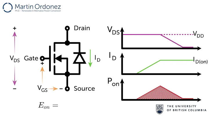
replied: The main parameters of MOSFET include BVDSS, RDS(on), Crss, Coss and VGS(th); the lower tube, half bridge and full bridge circuit of synchronous BUCK converter, as well as the secondary side synchronous rectifier tube of some isolation converters Parameters such as internal diode reverse recovery should also be considered, and should be combined with the specific application. The following waveform shows the process of turning on the inductive load power MOSFET.
Turn-on process of power MOSFET, reference:
Understand the switching process of MOSFET based on the characteristics of the drain conduction area, Electronics Today: 2008.11
Understand the switching loss of power MOSFET, Electronics Today: 2009.10
Switching loss of power MOSFET: Turn-on loss
Understand The switching process
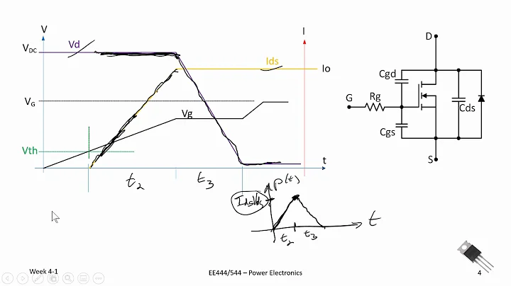
VGS(th) and VGP of the power MOSFET can be found in the data sheet of the power MOSFET. VGP is not marked in some data sheets, and the voltage value of the platform can be obtained through calculation. The time periods where turn-on loss occurs are t1-t2 and t2-t3. The time period t0-t1 does not produce turn-on loss but does cause delay. In the application of
load switch, it is necessary to ensure that after the t3 time, the charging of the output capacitor is basically completed, that is, the voltage of the capacitor is basically equal to the input voltage. During this process, MOSFEGT works in the linear region and controls the voltage VGP of the platform. It is equivalent to controlling the maximum surge current , and the surge current will not have an impact on the system. Therefore, the conduction time is determined by the output capacitance and load size. The specific calculation steps of
are: setting the maximum surge current Ipk, the maximum output capacitance Co and the output load Io during power-on. If the output is loaded after the output voltage is stable, then take: Io=0. The output capacitor charging time t can be calculated from the following formula. The application of
load switch usually connects external capacitors in parallel with D and G poles, so t2-t3 time is much longer than t1-t2, t1-t2 can be ignored, so we can get: t=t2-t3, D and G can be calculated by the formula Very parallel external capacitor value. Then the circuit is actually tested based on the above values to meet the design requirements. The steady-state power consumption of the
load switch is not large, but the transient power consumption is very large, especially when working in the linear region for a long time, thermal failure problems will occur. Therefore, in PCB design, especially for SMD MOSFETs, attention should be paid to fully laying copper sheets for heat dissipation. In the MOSFET data sheet, the thermal resistance is measured with the component mounted on a 1 square inch 2OZ copper circuit board. Drain copper is spread over the entire 1 square inch 2OZ copper circuit board. In actual applications, it is impossible to use a 1 square inch 2OZ copper circuit board for Drain's copper sheet. We can only use as large a copper sheet as possible to ensure thermal performance. Specific possible derating values can be found in the figure below. If it is a multi-panel, it is best to lay copper on each layer where the D and S poles correspond to the copper, and connect them with multiple vias. The size of the holes is about 0.3mm.
SO8 standard thermal resistance: RθJA=90C/W, RθJC=12C/W. SO8 copper package thermal resistance: RθJA=50C/W, RθJC=2.5C/W.
Question 2: What is the relationship between Qgs, Qgd, Ciss, Crss, Coss, tr and tf of power MOSFET?
reply: As shown in the figure below, under certain test conditions, Qgs is related to Ciss, Qgd is related to Crss, Qg is related to both Crss and Ciss, and the driving voltage determines its final charge value. Qgs and Qgd are calculated values based on the associated capacitance.
In recent years, the author has visited many customers and met a large number of engineers who are engaged in power supply design and development on the front line. During the communication with them, they also encountered many technical problems, and then we analyzed the results of these problems. reasons and find corresponding solutions. In this process, I have encountered confusion and confusion, and also experienced the joy of success, and have made promising friends with many engineers. They are the most solid happiness and wealth in my life. They have always encouraged me, and I will encounter many future challenges. Sharing my experience, I will now sort out some typical application issues of power MOSFETs, hoping to be helpful to the majority of electronic engineers.
Question 1: What are the main parameters to consider in the application of power MOSFET? In a load switch application, how to calculate its on-time? In PCB design, what is the best copper foil area? Do the copper foil areas of D and S poles need to be the same? Is there a formula to calculate it?
replied: The main parameters of MOSFET include BVDSS, RDS(on), Crss, Coss and VGS(th); the lower tube, half bridge and full bridge circuit of synchronous BUCK converter, as well as the secondary side synchronous rectifier tube of some isolation converters Parameters such as internal diode reverse recovery should also be considered, and should be combined with the specific application. The following waveform shows the process of turning on the inductive load power MOSFET.
Turn-on process of power MOSFET, reference:
Understand the switching process of MOSFET based on the characteristics of the drain conduction area, Electronics Today: 2008.11
Understand the switching loss of power MOSFET, Electronics Today: 2009.10
Switching loss of power MOSFET: Turn-on loss
Understand The switching process
VGS(th) and VGP of the power MOSFET can be found in the data sheet of the power MOSFET. VGP is not marked in some data sheets, and the voltage value of the platform can be obtained through calculation. The time periods where turn-on loss occurs are t1-t2 and t2-t3. The time period t0-t1 does not produce turn-on loss but does cause delay. In the application of
load switch, it is necessary to ensure that after the t3 time, the charging of the output capacitor is basically completed, that is, the voltage of the capacitor is basically equal to the input voltage. During this process, MOSFEGT works in the linear region and controls the voltage VGP of the platform. It is equivalent to controlling the maximum surge current , and the surge current will not have an impact on the system. Therefore, the conduction time is determined by the output capacitance and load size. The specific calculation steps of
are: setting the maximum surge current Ipk, the maximum output capacitance Co and the output load Io during power-on. If the output is loaded after the output voltage is stable, then take: Io=0. The output capacitor charging time t can be calculated from the following formula. The application of
load switch usually connects external capacitors in parallel with D and G poles, so t2-t3 time is much longer than t1-t2, t1-t2 can be ignored, so we can get: t=t2-t3, D and G can be calculated by the formula Very parallel external capacitor value. Then the circuit is actually tested based on the above values to meet the design requirements. The steady-state power consumption of the
load switch is not large, but the transient power consumption is very large, especially when working in the linear region for a long time, thermal failure problems will occur. Therefore, in PCB design, especially for SMD MOSFETs, attention should be paid to fully laying copper sheets for heat dissipation. In the MOSFET data sheet, the thermal resistance is measured with the component mounted on a 1 square inch 2OZ copper circuit board. Drain copper is spread over the entire 1 square inch 2OZ copper circuit board. In actual applications, it is impossible to use a 1 square inch 2OZ copper circuit board for Drain's copper sheet. We can only use as large a copper sheet as possible to ensure thermal performance. Specific possible derating values can be found in the figure below. If it is a multi-panel, it is best to lay copper on each layer where the D and S poles correspond to the copper, and connect them with multiple vias. The size of the holes is about 0.3mm.
SO8 standard thermal resistance: RθJA=90C/W, RθJC=12C/W. SO8 copper package thermal resistance: RθJA=50C/W, RθJC=2.5C/W.
Question 2: What is the relationship between Qgs, Qgd, Ciss, Crss, Coss, tr and tf of power MOSFET?
reply: As shown in the figure below, under certain test conditions, Qgs is related to Ciss, Qgd is related to Crss, Qg is related to both Crss and Ciss, and the driving voltage determines its final charge value. Qgs and Qgd are calculated values based on the associated capacitance.The rising and falling delays of
are related to Crss and Ciss, and the measurement condition is resistive load. If it is an inductive load, the current of the inductor cannot change suddenly, so due to the freewheeling of the inductor, this time is related to the characteristics of the load.
rise delay tr: The definition of rise delay is that during the turn-on process of MOSFET, the voltage of VGS rises, starting from its 10% value, until VDS drops to 10%VDS value. During the startup process, the time before VGS rises to the Miller capacitance plateau is determined by Ciss, the time before the Miller capacitance plateau is determined by Crss, and the time after the Miller capacitance plateau until VDS drops to 10% VDS is determined by Ciss. The fall delays tf and tr are defined similarly.
gate charge characteristics and resistive turn-on process of power MOSFET, reference:
Gate charge characteristics of power MOSFET
Resistive load switching characteristics of power MOSFET
Question 3: In the data sheet of AOD4126, the ID marked in red What is the difference between , IDSM and IDM? Are the values of PD and PDM mislabeled? In addition, regarding RθJA and RθJC, which one in the remarks should a user make a judgment on? For MOSFETs with the same specifications, what are the advantages of dual-channel compared with single-channel? Is it a simple synthesis of parameters such as halving RDS(on) and doubling ID?
replied: In the MOSFET data sheet, ID and IDSM are both calculated values. ID is calculated based on RθJC and RDS(on) and the maximum allowable junction temperature. IDSM is calculated based on RθJA and RDS(on) and the maximum allowable junction temperature. Obtained, PD and PDM are also calculated values based on the above conditions.
takes TC=25C when calculating, but in actual applications, TC often exceeds 100C, and because the heat dissipation conditions used by the devices are different, dynamic parameters must also be considered during the switching process, so it is meaningless to select MOSFET based on current derating, ID No practical meaning.
RθJA and RθJC are two different thermal resistance values. The specific definitions are detailed in the data sheet. The thermal resistance values in the data sheet are measured under certain conditions. Due to different conditions in actual application, The resulting measurements are not identical.
uses dual-channel and single-channel MOSFETs. Switching losses and conduction losses must be considered comprehensively. RDS(on) is not simply halved. Because the two power tubes work in parallel, the problem of imbalance will always exist, and dynamic switching It is easy to produce dynamic imbalance in the process. If switching losses are not considered and only conduction losses are considered, RDS(on) still needs to be derated to a certain extent.
Current definition of power MOSFET, reference:
Functional analysis of the current of power MOSFET, Electronics Today: 2011.11
Understanding the current of power MOSFET tube
Thermal resistance characteristics of power MOSFET
Question 4: Different test conditions affect the data of MOSFET VGS(th) and BVDSS in the table? How is ATE determined?
replied: The results will be different under different test conditions, so detailed test conditions will be marked in the data sheet to make the test results repeatable. For AET testing, take VGS(th) as an example. It is related to Igss. For example, AON6718L, when the maximum voltage of 20V is applied to the G and S poles, VDS=0V, and Igss is less than 100nA, it means the test has passed.
Different companies such as ST, Fairchild, IR, Vishay, etc. may use different Igss, such as IR1010 using 200nA and IR3205 using 100nA. Currently, 100nA is more commonly used in the industry. BVDSS test conditions: ID=250uA, VGS=0V, some companies use 350uA, 500uA or even 1mA. The larger the ID, the higher the BVDSS voltage value.
Specific test conditions for power MOSFETs, reference:
Overlooked details: Understanding MOSFET voltage ratings BVDSS
Understanding MOSFET VTH: Will gate-induced voltage spikes cause shoot-through damage?
The power supply system does not turn on at low temperatures. Have you ever encountered this: Understanding the VTH temperature coefficient
Question 5: For a 100V MOSFET, the VGS withstand voltage can only reach 30V. When the device is turned off, VGD can reach about 100V. Is it because the thickness of the gate oxide layer between the G and S electrodes is relatively thick, or is the voltage drop mainly due to the sinking and drift resistors?
replied: The voltages of G and S are mainly controlled by the thickness of the gate oxide layer, and the voltages of G and D are mainly controlled by the thickness of the epitaxial layer EPI+ layer, so VGD has a high withstand voltage.
Question 6: Regarding avalanches, is the following description correct?
1. Will a simple overvoltage damage the MOSFET?
replied: In many cases, 1,000 pieces or 10,000 pieces are measured. If the voltage is higher than the rated voltage value, the MOSFET will not be damaged. The power MOSFET has certain avalanche resistance.
2. There are two situations of avalanche damage to MOSFET: one is a fast high-power pulse, which directly causes the parasitic diode to generate a large avalanche current, and the chip is quickly heated and overheated and damaged. The other is that the parasitic transistor is turned on and secondary breakdown occurs?
replied: Yes, especially the MOSFETs of the new generation process are basically damaged in the latter way: the parasitic transistor is turned on. The conduction of the parasitic transistor and the occurrence of secondary breakdown are not all due to the occurrence of avalanche, but may also be caused by excessively high dv/dt.
3 and avalanche damage all occur when the VDS is greater than the rated value ?
replied: Yes. However, under high temperature conditions, when some large currents are turned off, the parasitic transistor may be turned on and damaged during the turn-off process. Although overvoltage is not seen, the author still defines it as avalanche UIS damage.
4. Regarding the two situations in (2), under what circumstances is the first one likely to occur, and under what circumstances is it likely that the second one will occur?
reply: If the cells are very consistent, the heat dissipation is very good and even, and the thermal balance is good, the first situation occurs, and this damage mode is sometimes seen in early planar processes. Nowadays, the new technology leads to the increasingly concentrated density of units, and the damage caused is usually caused by the second type.
The parasitic transistor in the body is turned on and causes avalanche damage. At the same time, the parasitic transistor in the body undergoes secondary breakdown. At this time, the collector voltage is reduced to 1/2 of the withstand voltage within 1-2 n seconds of the transient time. The reason is that Avalanche injection of carriers occurs in the internal depletion layer, and the electric field current density is very large, close to the critical electric field of the silicon wafer. The current is large, the voltage is high, the electric field is large, and the ionization is strong. A large amount of hole current flows through the base area P body resistance RB, the parasitic transistor is turned on, and the collector voltage quickly returns to the breakdown voltage when the base is open circuit. When the gain is large, avalanche breakdown occurs in the triode, and this withstand voltage value is low. Conditions for avalanche injection in
transistors: electric field stress, forward bias thermal instability. When the
MOSFET is turned off, the channel drain current decreases, and the inductive load increases VDS to maintain a constant ID current. The ID current consists of the channel current and the displacement current. The displacement current is the body diode depletion layer current and is proportional to dV/dT. The increase in VDS is related to the base discharge and drain depletion layer charging speed. The charging speed of the drain depletion layer is related to the capacitance Coss and ID. The larger the ID, the faster the VDS rises. The drain voltage rises, the body diode avalanches to generate carriers, the entire ID current avalanches through the diode, and the channel current is 0.
UIS characteristics of power MOSFET, reference:
Understanding the UIS of power MOSFET, Electronics Today: 2010.4
Many engineers ask this question: If the UIS is damaged by avalanche, the voltage will usually reach 1.2~1.3 times of the withstand voltage value. , you can clearly see that the voltage is clamped, which in popular terms means the waveform is cut off. So is it safe for a 100V device to operate at 105V or 110V? As mentioned above, 100V devices will not be damaged by adding 110V voltage. So what are the safety principles?
For design engineers, what is required is that the design parameters have a certain margin under the most extreme conditions, that is, from a design perspective, maintaining the safety and reliability of the system is always the highest priority. . Therefore, the principle suggested by the author is: the transient voltage peak should not exceed the rating of the MOSFET under dynamic extreme conditions.
Question 7: Regarding Trench MOS SOA, I heard that MOSFET has negative temperature coefficient effect in the amplification area, so it is easy to generate hot spots. Is this the second breakdown of the MOSFET? However, according to the data, the RDS(on) of the MOSFET has a positive temperature coefficient effect and will not cause a second breakdown. I have never understood this. Can you give me some advice? I will ask for details later.
replied: Both planar process and Trench process MOSFETs have this feature, which is an inherent characteristic of MOSFETs.The positive temperature coefficient effect of RDS(on) only has such characteristics under the steady-state condition of complete conduction, which can achieve steady-state current sharing. During the dynamic turn-on process, the
MOSFET will cross the negative temperature coefficient area and enter the fully turned-on positive temperature coefficient area; during the turn-off process, it will cross the fully turned-on positive temperature coefficient area and enter the negative temperature coefficient area. Just because the unit density of the planar process is very small, the possibility of local overcurrent and overheating is small, so the thermal balance is good. In contrast, the thermal shock resistance is good when dynamically passing through the negative temperature coefficient zone. Usually, this area should be passed quickly during the design process to reduce the occurrence of thermal imbalance.
RDS(on) characteristics of power MOSFET, reference:
Understanding the RDS(on) temperature coefficient characteristics of power MOSFET, Electronics Today: 2009.11
Selection of medium-voltage power MOSFETs applied to linear regulators, Electronics Today: 2012.2
Power The influence of MOS tube RDS(on) negative temperature coefficient on load switch design, Electronic Technology Application: 2010.12
Understand the RDS(on) negative temperature coefficient characteristics of power MOSFET
Question 8: Regarding parasitic diodes and transistors, is the following understanding correct? In the figure below, the S pole is not in direct contact with the P-type layer, so there is no parasitic diode, only a parasitic transistor. However, this triode is easy to mislead, so the P-type layer is also directly connected to the S-stage to weaken the triode effect. So it is manifested as an obvious parasitic diode at this time?
replied: Yes, the above understanding is correct. At present, the S pole of the power MOSFET is connected to P+, and the unconnected structure as shown in the picture is rarely used. The main reason is: for the internal parasitic transistor, connecting the S pole and P+ together is equivalent to a short circuit between the base and emitter stages, and not connecting them together is equivalent to an open circuit. The VCBOVCEO of the triode thus increases the withstand voltage of the power MOSFET. In this way The internal connections also result in internal parasitic diode functions connected to external circuitry.
Question 9: Regarding the Miller capacitance Crss, in the document Dynamic Parameters of MOSFET, there is a formula as shown in the reference picture. The Crss capacitance is the capacitance of the gate through the oxide layer to the drain. For the switching process, in the second stage, the channel is open Finally, why was Ciss added? What is the reason? In addition, the test condition in the AON6450 specification sheet is VDS=50V. What is the reason for this test condition? Can you give the capacitance value under other conditions?
replied: The reason why Ciss increases is that Crss increases. After the device in the figure is turned on, Wdep decreases and Crss increases. For a 100V device, such as AON6450, due to the Miller platform area, VGD will drop from 100V to less than 10V in the extreme case.
Coss and Crss are dynamic capacitors. The capacitance changes with VDS, and the relationship is not linear. The test conditions used in the data sheet are the standards commonly used in the industry, testing at 50% VDS. If customers have special requirements, 80% or 100% of the data can be provided.
Capacitance characteristics of power MOSFET, reference:
Understanding the parasitic capacitance of power MOSFET
Understanding the Coss loss of power MOSFET
Question 10: How is the SOA curve of power MOSFET obtained? Can it be used as a safety standard for design?
replied: The SOA curve of any company mainly consists of three parts: the resistance limitation area, several current and voltage straight lines limited by pulse power, and the maximum voltage straight line. The maximum voltage value is the rating in the data sheet. Several current and voltage straight lines limited by pulse power are actually calculated values, which are calculated based on the transient thermal resistance, on-resistance and maximum allowable junction temperature in the data sheet, and are all based on TC=25 degrees. TC represents the temperature of the exposed copper of the package. In actual applications, the temperature of TC is much higher than 25 degrees. Therefore, the SOA curve cannot be used as a design verification standard.SOA definition of
power MOSFET, reference:
power MOSFET safe operating area SOA: Is it really safe?
Question 11: If VGS is greater than VGS(th), the MOSFET is turned on, and the MOSFET has just entered the Miller platform, is it considered saturated? If so, stop supplying power to the G electrode at this time. Assuming that the leakage of the gate oxide layer is ignored, will VDS always maintain a relatively high voltage drop? It feels a bit incredible, because after saturation, RDS(on) has dropped. If there is no saturation, it doesn't make sense. RDS(on) is related to VGS. After reaching 10V, RDS(on) is already very small, and the voltage drop should also decrease. If the voltage drop will automatically decrease, does that mean that the later charging of the Miller platform is useless?
replied: When VGS is greater than VGS(th), the MOSFET starts to conduct. At this time, the current is very small. From the time it is turned on to when it first enters the Miller platform, the MOSFET works in the amplification area, and the device is not fully turned on. At this time, the MOSFET conducts The pass resistance is very large, and the voltage of the D pole is borne by the entire MOSFET, so the current is small. The current multiplied by the resistance is also equal to the VDS value, which is the power supply voltage value applied to the D and S poles. When the
MOSFET works in the linear region, it works on the same principle as a linear voltage regulator, that is, an LDO, such as the LM7805. For example: when the input voltage is 10V, the output is 5V, and the voltage drop is 5V; when the input voltage is 12V, the output is still 5V, and the voltage drop is It is 7V, and the MOSFET is equivalent to a regulating tube. The difference between the input voltage and the output voltage is borne by the MOSFET. When it reaches the Miller platform area, the current is the maximum current of the system, and the current cannot increase anymore. Then, the voltage of VDS begins to drop. Even if the voltage of VDS drops a little, the resulting voltage change rate is very large, so the current of the drive circuit , will all be extracted by the Miller capacitor Crss. At this time, the so-called "Miller plateau" is seen. The voltage of VDS maintains a stable value for a certain period of time until VDS completely drops to the minimum value, and the voltage of VDS changes. The Miller platform zone ends when the rate is 0.
Question 12: 1. Ask a question about AO3401A: Now the on-resistance RDS(on) of AO3401A is used as an isolation resistor to buffer the instantaneous impact current of hot-plugged mobile hard disk to prevent the main core voltage from being instantly lowered. The circuit diagram is as follows , 5V_USB is where the mobile hard disk is plugged in, and +5V_Normal comes from the main core voltage. The VGS is designed to be fixed at around -1.6V. The RDS(on) at this time is about 100mΩ. When the mobile hard disk is plugged in, the impulse current drops from the original 9A to about 5A. The impulse current lasts about 80 microseconds. The effect is Obviously, the current of the mobile hard disk is about 300mA when it is working normally. If VGS is designed to be around -2.5V, RDS(on) is only a few tens of mΩ, which has little effect on suppressing the inrush current. What are the design principles of this circuit?
replied: When VGS=-1.6V, the MOSFET can be guaranteed to be turned on. Pay attention to the dispersion of the resistor value. Under the worst conditions, if the accuracy of the resistor used is 10%, the absolute value of the VGS voltage: 1.3+1.6 *20%=1.64V, MOSFET can still work. If the accuracy of the resistor is 15%, considering the dispersion of the VGS(th) voltage of the MOSFET, the MOSFET may not work under certain conditions such as low temperature. Moreover, the VGS(th) voltage has a negative temperature coefficient, and the lower the temperature, the greater its value. The stable value of the
driving voltage must be combined with the most extreme conditions such as the minimum value of the input voltage and the accuracy of the voltage dividing resistor value, the temperature coefficient of VGS(th) and VGS(th), to select the appropriate voltage dividing ratio of the dividing resistor. , to ensure the design requirements of the system. When designing the PCB layout, both S and D are connected with large copper sheets. If it is a multi-layer board, put a copper sheet of corresponding size on each layer and connect it with multiple 10-15mil via holes for heat dissipation. The VGS(th) specification book of
2 and AO3401 states that it can reach -1.3V. If VGS=-1.6V is set, the absolute value of the voltage is greater than -1.3V. Is the MOSFET conducting normally? There should be no problem, right? Now losses are not a concern, the 0.03V drop in RDS(on) has no effect on the system. Originally, a 0.1 ohm oxide film resistor was used for isolation, but the resistor was too large. The purpose of using this circuit is to replace this resistor.In this circuit, the MOSFET is always on after the TV is turned on. The MOSFET is always on when the mobile hard disk is inserted, instead of inserting the mobile hard disk and then turning on the MOSFET. Therefore, I feel that adjusting the values of R45/R46/C18 will not work. to reduce the impact current. It is hoped that the constant current region characteristics of MOSFET can be used to reduce the inrush current. If VGS is adjusted to above -2.5V, the limiting effect on the inrush current will be very small, and can only be reduced from 9A to about 8A. This approach is not good for MOS. Will there be any problems?
replied: The above circuit is beneficial for the MOSFET to work in the linear area (amplification area, that is, the constant current area) for a long time during the turn-on process, thereby controlling large transient loads during power-on, such as hot-swappable mobile hard disks, because The hard disk has a large capacitive load, which causes a large surge current at the moment of cut-in. If the MOSFET is already turned on and a large capacitive load such as a mobile hard disk is inserted later, the surge current is mainly provided by the large capacitance at the output end, so the MOSFET cannot limit the surge current. When the
MOSFET works in the linear region, the resistance is much greater than the resistance when it is fully turned on, so it can also be understood as using a resistor to suppress the surge current. Usually when designing this kind of load switch circuit, the voltage dividing resistor is to prevent the maximum voltage of VGS from exceeding the rated maximum voltage, and the resistor connected in series to the G pole adjusts the turn-on speed of the MOSFET. Under the condition of ensuring the required turn-on speed and VGS cannot exceed the maximum rated voltage, the resistance value can be appropriately increased, so that under normal working conditions, the static loss generated after the MOSFET is fully turned on is reduced.
3. It is written on page 1 of the AO3401 specification that operation with gate votages as low as2.5V does it require that the G electrode voltage must be greater than 2.5V? VGS must be less than -2.5V? Is there any problem with the design VGS=-1.6V? What if we continue to increase VGS to -1V? The size of VGS does not matter, as long as the power consumption generated by RDS(on) does not cause the MOSFET to overheat, is that correct?
replied: You can’t think so. The meaning of this sentence is: AO3401 can work at VGS=-2.5V, and the on-resistance is about 120mOhm at this time. If the VGS voltage is too small, lower than the threshold voltage VGS(th), the AO3401 may not be fully turned on and may not work properly. It is still recommended to design VGS above -2.5V, such as around -3.5V, and reduce the inrush current by adjusting (increasing) R45/46 and C18.
Question 13: Using the following circuit, the GPIO port of the CPU is used to directly control a MOSFET tube, and the MOSFET is used as a switch for the back-end load. What are the risks of this application?
replied: Check VCC and the voltage value VGS after MR34/MR35 voltage division. The absolute value of VGS must be higher than the VGS(th) of MQ1 to ensure that the MOSFET is fully open, otherwise the subsequent system may not work; also check the driving capability of the GPIO port , whether it meets the driver's requirements. If it is small, it is best to use the GPIO port to drive the B pole of a triode, and the collector C of the triode pulls down the G pole of the MOSFET.
re-adjusts the MC11 value, as well as the MR34/MR35 value, based on the actual inrush current. During PCB design, D and S of MQ1 are connected with large copper sheets. If the board is multi-layer, put copper sheets on multiple layers and use multiple via holes to connect them respectively.
Question 14: I would like to ask a question about the DS voltage oscillation when the MOSFET is turned off. I tested two 30V MOSFETs from different manufacturers on the same circuit and obtained different DS voltage waveforms when turned off, as shown in the figure below. It can be seen that the peak of device 1 is higher, but the oscillation is suppressed quickly; the peak of device 2 is lower, but the oscillation is suppressed slowly. Because it is measured on the same PCB, the parasitic inductance, resistance and other parameters of the circuit remain unchanged. Now only the components are different. This spike is caused by the parasitic inductance on the circuit and the capacitance resonance of the MOSFET, but it is not clear which parameter difference between the two devices makes this oscillation behave so differently.Is it possible to select a MOSFET that has a lower peak value for actual applications and can quickly eliminate oscillations based on some parameter comparisons of device data?
reply: Such an oscillation waveform is often seen by a power supply engineer. Let’s first talk about the measurement method:
(1) Just like measuring the ripple of the output voltage, all engineers know that it is necessary to remove The cap of the oscilloscope probe directly contacts the signal tip of the probe and the ground wire at both ends of the measured location, reducing the loop of the ground wire, thereby reducing the spatially coupled interference signal.
(2) Bandwidth problem. When measuring the output voltage ripple, a bandwidth of 20MHZ is usually used. However, when measuring the VDS voltage of a MOSFET, what bandwidth is the correct measurement method? In fact, if different bandwidths are used, the amplitude of the measured spike voltage is different.
The specific principles are: ① Determine the fastest rise Tr and fall time Tf of the measured signal; ② Calculate the highest signal frequency: f=0.5/Tr, Tr takes 10%~90% of the measured signal; f=0.4/Tr, Tr takes 20%~80% of the measured signal; ③ Determine the required measurement accuracy, and then calculate the required bandwidth.
In the waveform above, the fastest falling time of the measured signal is 2ns (10%~90%). Determine the minimum bandwidth required by a Gaussian response oscilloscope when measuring the measured digital signal: f=0.5/2ns=250MHz . If a 3% measurement error is required: the required oscilloscope bandwidth = 1.9*250MHz = 475 MHz; if a 20% measurement error is required: the required oscilloscope bandwidth = 1.0*250MHz =250MHz. Therefore, an important factor in determining the bandwidth of an oscilloscope is: the fastest rise time of the signal being measured. Note: The system bandwidth of an oscilloscope is determined by both the oscilloscope bandwidth and the probe bandwidth. System bandwidth of
Gaussian frequency response: (oscilloscope bandwidth 2 + probe bandwidth 2) 1/2/2
Maximum flat frequency response system bandwidth: min (oscilloscope bandwidth, probe bandwidth) The oscillation waveform of
VDS is caused by the PCB parasitic loop inductance and MOSFET parasitic The capacitor forms high-frequency resonance. Under the condition that the parasitic inductance value is certain, the smaller the parasitic capacitance, the higher the frequency of oscillation and the higher the amplitude. At the same time, the amplitude of oscillation is related to the initial current value of the loop.
pay special attention to the fact that the parasitic capacitance Coss is not linear and decreases as the voltage increases, so it can be seen that the frequency of waveform oscillation is not fixed. The high-frequency oscillation of VDS cannot be eliminated. Adding Coss or connecting external parallel capacitors on the D and S poles can reduce the frequency and amplitude of the oscillation. The Snubber circuit also uses this principle to suppress voltage spikes.
Question 15: Why does the withstand voltage of power MOSFET have a positive temperature coefficient? The temperature is high and the withstand voltage of the power MOSFET is high. Does that mean that the MOSFET has a greater margin to voltage spikes and that the MOSFET is safer?
replied: As the temperature increases, the thermal vibration of the crystal lattice intensifies, causing the mean free path of carrier movement to shorten. Therefore, the energy obtained by the external electric field acceleration before colliding with the atoms is reduced, and the possibility of impact ionization is also reduced accordingly. In this case, avalanche breakdown can occur only by increasing the reverse voltage and further enhancing the electric field. Therefore, the avalanche breakdown voltage increases with temperature and has a positive temperature coefficient. The measurement of
MOSFET withstand voltage is based on a certain drain current. When the temperature rises, in order to achieve the same measured drain current, the only way is to increase the voltage. On the surface, it seems that the measured withstand voltage has increased. However, the ultimate cause of MOSFET damage is temperature. More often, it is local overtemperature, which leads to local overheating damage. When the overall temperature increases, MOSFET is more likely to have thermal and current imbalance in the unit, leading to damage.
Question 16: Use the circuit in the figure below to convert between different level signals. VCC_SIM=5V, SIM_DATA and SIM_CARD_I/O belong to I/O bidirectional transmission. SIM_DATA is the input signal. It can be understood that when SIM_DATA is high, Q7 is cut off, and SIM_CARD_I/O receives a 5V signal; when SIM_DATA is low, Q7 is turned on, and SIM_CARD_I/O receives a low-level signal.When SIM_DATA is an output signal, how to understand that the SIM_CARD_I/O input is a low-level signal?
replied: The current of the power MOSFET can be from D to S, or from S to D, but from S to D is uncontrollable. At this time, the parasitic diode in the body is turned on. When a power MOSFET is used as a synchronous rectifier, the parasitic diode is usually turned on first, and then the gate signal drives the MOSFET to turn on: channel conduction to reduce conduction losses. When
SIM_DATA is the output signal, SIM_CARD_I/O is low level, the parasitic diode in Q7 is turned on, the signal SIM_DATA is also pulled low, and the low level signal is received. When SIM_CARD_I/O outputs a high level of 5V, the parasitic diode in Q7 is cut off, and the signal SIM_DATA is pulled up to 3.3V to receive a high level signal.
Question 17: Why is the UIS avalanche capability of superjunction high-voltage power MOSFET lower than that of planar technology?
reply: The superjunction structure penetrates into the bottom P region, increasing the complexity of the process. It is difficult to fully control the symmetry of the middle depletion layer and the lateral electric field, and local electric field concentration is prone to occur.
Working principle of super junction power MOSFET, reference:
Understanding the MOSFET switching process based on the characteristics of the drain conduction area, Electronics Today: 2008.11
High voltage super junction Super Junction structure and working principle
Question 18: What are the damage modes of power MOSFET? ? How to tell how a MOSFET is damaged?
replied: Mainly damage caused by ESD, overvoltage, overcurrent and overtemperature.
Damage modes of power MOSFET, reference:
Damage mode and analysis of power MOSFET in switching power supply, Electronic Technology Application: 2013.3
Question 19: Why are there two different ratings of dv/dt in the data sheet of power MOSFET? How to understand the specific dv/dt of body diode reverse recovery?
replied: In the flyback power supply, when the primary side main switch is turned off, the VDS waveform starts to increase from 0, so a certain slope dv/dt is generated, and a voltage spike is generated at the same time, which is the inductance of the parasitic circuit and the MOSFET Formed by parasitic capacitance oscillation. This dv/dt will usually be coupled to the gate through Miller capacitance, generating a voltage on the gate. If the gate voltage is greater than the threshold voltage, the MOSFET will be misdirected and damaged, so it is necessary to limit the dv/dt during the turn-off process of the MOSFET. .
Another situation is that in LLC, half-bridge and full-bridge circuits, and the lower tube of synchronous BUCK, after the lower tube is turned off, the parasitic diode of the lower tube first conducts freewheeling, and then the corresponding upper tube of the upper arm is turned on, and the diode DV/DT problems can also occur during reverse recovery. Typically the dv/dt rating of a diode's reverse recovery is much smaller than the dv/dt rating of the MOSFET itself. During the reverse recovery process of the
diode, if the stored charge is not completely cleared, the diode, that is, the lower tube cannot withstand the voltage drop. The lower tube is equivalent to a short circuit. Then during the process of turning on the upper tube, the voltage of the power supply can only increase. On the stray inductance of the loop: If the lower tube is short-circuited, the input current will increase sharply. The stray inductance of the loop will limit the current increase. Therefore, the voltage of the power supply can only be added to the stray inductance of the loop. The longer this process lasts. , the greater the short-circuit current impact, the MOSFET may be damaged during the reverse recovery process of the diode. As for whether the upper tube or the down tube is damaged, it depends on the impact resistance of the power.
Reverse recovery of power MOSFET diode, reference:
Understanding the reverse recovery characteristics of power MOSFET body diode, Electronics Today: 2012.11
Question 20: AOD2922 is used in the BOOST circuit LED backlight driver, and one of the MOSFETs is found to have failed, G, D , S is short-circuited. After continuing to work for some time, D and S become open-circuited again. Why?
replied: The initial failure occurred inside the silicon wafer. It should be the breakdown of internal D and G, resulting in short circuit of G, D, and S. After continuing to work for some time, due to the impact of large current, the connection between S and the silicon wafer was caused. Melting and burning are disconnected, so D and S are open circuits.
Question 21: In applications, the Miller platform may drop. Is there a risk if it drops below the turn-on voltage?
replied: If it is a flyback single-tube operation, DCM has no effect. If it is a flyback CCM, the system is prone to instability and affects the safety of the MOSFET.If multiple PFC tubes work in parallel, the MOSFETs cannot share the current well during the turn-on process, and the risk of damage is high.
question 22: In some applications, several MOSFETs are commonly connected in parallel for current expansion or heat dissipation. When a protected power supply is used to debug the system and a circuit problem occurs accidentally, only one tube will burn. How to determine which MOSFET is damaged?
replied: Use a multimeter on the electrical barrier to detect the voltage of D-G of each MOSFET. Connect the red pen to D. The MOSFET with the smallest resistance is the damaged one.
Question 23: The 480W isolated power module uses a primary-side full-bridge rectifier. Module input voltage is 51V~56VDC, rated output is 10.8V, 48A. What broke this time was two pipes on one bridge arm. During application, abnormality of the peripheral circuit causes the secondary side current to flow back into the primary side rectifier, and the current flows from Source to Drain. Combined with the burn traces on the source surface in the FA report, the cause analysis is the EOS of the current. Can it be proved that the source is burned because the current flows from S to D?
replied: For synchronous rectification, the output backfeed current is the worst condition. During the design process, the output backwash current should be reduced as much as possible.
(1) The output backfeed causes an avalanche of the output rectifier, causing damage to the output synchronized rectifier. This depends on the avalanche capability of the output synchronized rectifier and the magnitude of the negative current formed by the backfeed current.
(2) The output reverse current will affect the operation of the primary MOSFET.
When the output forms a reverse current, if Q1 and Q2 are a half-bridge arm, Q1 is the upper tube and Q2 is the lower tube; Q3 and Q4 are another half-bridge arm, Q3 is the upper tube and Q4 is the lower tube; If the full-bridge phase-shift soft switching is not used but PWM hard switching, since the output is a reverse current, before Q1 and Q4 are turned on, the current will flow from the Q1 and Q4 diodes; when Q1/4 is turned on, the current will flow from Q1 and Q4 channels flow through. When the energy of the secondary output inductor is large enough, its primary current is not enough to reverse direction. Therefore, after Q1 and Q4 are turned off, the current still has to flow through the Q1 and Q4 diodes. After the dead time, Q2 and Q3 are turned on. At this time, due to the long current flowing through the Q1 and Q4 diodes, the current is relatively large, and the dead time is short. For some MOSFET diodes, the reverse recovery time is not enough, or the Q1 and Q4 body diode charges are not fully recovered. At this time, Q2 and Q3 are turned on, which will cause the upper and lower bridge arms to be connected until they are damaged.
As for whether the upper bridge or the lower bridge is damaged, it depends on which tube has a stronger ability to withstand a short circuit. Whether to damage the primary side or the secondary side depends on which side of the pipe has greater capacity.
-- For the secondary side, it is the voltage avalanche after the large current is turned off.
-- For the primary side, the diode reverse recovery causes high current damage to the upper and lower bridges.
(2) Generally, diodes also have a negative temperature coefficient, which causes damage similar to the damage caused by the accumulation of heat in the linear region during turn-on, which corresponds to the MOSFET form in which the diode has not fully recovered. Therefore, for this example, the best way, from a design perspective, is to reduce the output backfeed current. From the device perspective, improving the reverse recovery characteristics of the body diode of the primary MOSFET can improve the safety of the primary device. The final method is to control the output reverse current to truly maintain system security.
Question 24: When the MOSFET voltage is measured, the current is 250uA, but the IDSS current in the data sheet is only a few uA. Why?
replied: The IDSS current is small, indicating that the actual leakage current is less than the requirements of the test specification, so it is qualified.
Question 25: After the MOSFET is damaged, the impedance changes to an intermediate value, sometimes working and sometimes not working, why?
replied: Usually after the MOSFET is damaged, if the power supply does not have current protection, a larger current impact will cause the internal metal wires to melt and vaporize. After the system does not work, the MOSFET cools down, the melted and vaporized metal solidifies, and local areas are connected to form a larger impedance. After the MOSFET is powered on, these local connected areas are disconnected, and the MOSFET stops working. Sometimes this phenomenon also occurs: the internal metal is disconnected after cooling and solidification, and the metal melts after electricity is applied, causing the internal areas to be connected.
Question 26: When testing the reverse recovery of the diode in the high-voltage MOSFET body, the lower the IF, the larger the Qrr, and the higher the voltage spike, why?
replied: When the MOSFET's body diode conducts, charges accumulate at the PN junction, and these charges are removed when the diode begins to experience blocking voltage. If the IF is low, the level of charge accumulated in the PN junction is low and the speed of removal is fast, the dv/dt is large, and the offset current of C*dv/dt is large. The tested Qrr includes the true Qrr as well as the minority carrier associated with C*dv/dt, so the tested Qrr is larger when IF is low.
Question 27: The customer uses an external signal to control the pin ID of the PMIC. The PMIC is powered by a battery. The ID pin is internally pulled up by a 10M resistor and connected to the battery. When the external signal is 0, the 300K external resistor needs to be connected to the ID. pin; when the external signal is 1, the 300K external resistor and the ID pin are disconnected. How to achieve this?
replied: Use two AON1605, as shown in the figure, R1 is the internal pull-up resistor of the ID pin of the PMIC, R2 is the external 300K resistor, V_driver is the external control signal, when V_driver is 0, Q2 is turned off and Q1 is turned on. ID is pulled down to ground by a 300K resistor. When V_driver is 1, Q2 is turned on, Q1 is turned off, and ID is pulled up to the battery by the internal 10M resistor. At this time, R3 produces static loss. The larger R3 is, the smaller the power consumption is. When Q1 is turned on, the S pole voltage of Q1 is: 3.8V*300K/(10M+300K) =0.11V.
Question 28: Is the temperature coefficient of the power MOSFET capacitor a positive temperature coefficient or a negative temperature coefficient?
replied: The capacitance of power MOSFET does not change with temperature within the normal temperature range of 500K, especially Ciss, Cgs and Crss(Cgd).
Coss (Cds+Cgd) is composed of both Cgd and PN junction capacitance of MOSFET. If the temperature is too high, close to the intrinsic temperature of silicon, the concentration of intrinsic semiconductor carriers will increase a lot, and the capacitance of PN junction will increase. The temperature The simulation results of increasing from 300K to 600K are shown in the figure.