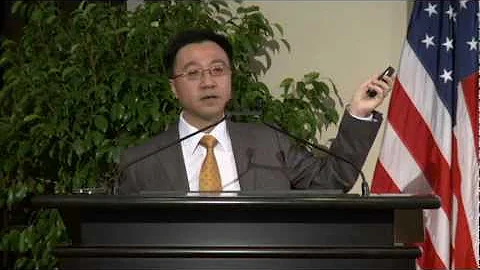
The inauguration ceremony in the United States has just ended. TSMC held the mass production and expansion ceremony of the Nanke 3nm plant today. Heavyweight guests were present, including Minister of Economic Affairs Wang Meihua, TSMC Chairman Andy Lau, etc. were present. Liu Deyin also revealed at the ceremony that 2nm's projects in Hsinchu and Taichung are in progress as scheduled.
Nanke is the main base for TSMC's 3nm production capacity . The foundry that will be expanded is the Fab18 factory area, which mainly produces 3nm and 5nm chips. Since TSMC rarely held ceremonies when inaugurating advanced process plants in the past, today's rare official announcement has attracted attention from all walks of life.
Sources pointed out that TSMC has taken the unusual step of inviting its suppliers and customers, as well as the media, to attend the upcoming 3nm process mass production launch ceremony on December 29. This pure wafer foundry has never held such a launch event before to showcase its latest process technology.
TSMC’s 3nm revenue exceeds 5nm, and the second phase of the US factory will also start construction
Liu Deyin said in his speech: "3nm and 5nm have similar yields during the same period, and customers have jointly developed new products and mass-produced them." Compared with 5nm technology, 3nm density increases by 60%, and power consumption is reduced by 30%-35% at the same speed, TSMC pointed out : "This is the most advanced technology in the world."
TSMC's biggest rival Samsung announced mass production of 3nm in June this year. Although it seems to be one step ahead of TSMC, many semiconductor analysts have said that so far they have not seen Samsung's yield figures for the 3nm part, and they are quite skeptical about the quality of mass products.
Regarding revenue contribution, Liu Deyin pointed out that the mass production of 3nm will generate annual revenue greater than 5nm, "within 5 years, the value of end products will be US$1.5 trillion around the world." He added that 3nm technology will be widely used to promote future top products, including supercomputers, data centers, high-speed Internet, mobile devices, and AR/VR.
In addition, Andy Lau also further announced TSMC’s factory expansion blueprint. In addition to the opening of the R&D center in Hsinchu in the second quarter of 2023, which is expected to employ 8,000 TSMC R&D personnel; 2nm will also be located in Hsinchu and Taichung Science Park respectively. "There will be a total of six phases of projects, and they are now underway as planned."
Liu Deyin also revealed that TSMC's second phase of construction in the United States will also be launched simultaneously to win the trust of customers and increase TSMC's future growth momentum.
Liu Deyin said that all factories in TSMC Nanke are green buildings and will achieve the target of 60% replacement rate of recycled water in 2030, and achieve 100% renewable energy replacement and net zero carbon emissions in 2050.
"De-Taiwanization" does not exist
The recent issue of "de-Taiwanization" has caused widespread discussion. Liu Deyin also emphasized again: "TSMC will continue to maintain its technological leadership, deeply cultivate the Taiwan region and continue to invest." He also pointed out that today's 3nm development and mass production achievements of TSMC are the result of joint cooperation with the local supply chain and channels in Taiwan, China. "Nikkei Asia" also pointed out that more than 90% of TSMC's production base is still in Taiwan.
Liu Deyin predicts that Fab18 is a very large factory. Today's start is to enter the eighth phase of expansion, each of which includes a large clean room with an area of 58,000 square meters. Liu Deyin said that each phase of the super-large factory is twice the size of a standard logic circuit factory.
Liu Deyin said that all factories in TSMC Nanke are green buildings and will achieve the goal of 60% replacement rate of recycled water by 2030, and achieve 100% renewable energy replacement and net-zero carbon emissions by 2050.
TSMC 3nm process variants
While improving the production yield of N3, TSMC has developed multiple 3nm process variants to meet customers' different needs for chip performance, power, chip size and cost. Company CEO Wei Zhejia has stated at company events many times that 3nm will be another large and lasting node for TSMC.
TSMC’s 5nm, 7nm and 28nm are also large and persistent nodes for foundries, with each process family containing three or more variants.
TSMC is about to put N3 into mass production and plans to launch an enhanced version of N3 - N3E in the second half of 2023. Two other 3nm process variants - N3P and N3S - will launch in 2024, followed by N3X in 2025.
Samsung Electronics may have defeated TSMC in the GAA process race, with the former claiming that its 3nm process node using gate-all-around transistor architecture has begun mass production earlier this year. TSMC's 3nm process family still uses FinFET (FinFET) technology and has begun expanding its customer base even before it is ready for mass production, sources said.
Samsung 3nm customer
Samsung announced the start of 3nm chip production in June 2022, and has taken a technological leadership position with the world's first GAA process. However, sources note that Samsung has not signed any significant 3nm chip customers. In addition, sources said that Samsung lost part of its 5/4nm chip business to TSMC, and TSMC has regained large orders from Nvidia and Qualcomm .
Samsung has also failed to secure orders for Qualcomm’s 5G modems and radio frequency chips due to be launched next year. TSMC secured the order for its 5nm and 7nm process families.
Meanwhile, disappointing sales of Android smartphones, including Samsung's Galaxy smartphones, have adversely affected shipments of its own Exynos chips, sources said. Samsung may ultimately find it difficult to accelerate the return on investment (ROI) of and made on its sub-7nm process.
In addition, Samsung’s foundry capital expenditures still lag far behind TSMC. TSMC has revised its 2022 capital expenditure outlook to $36 billion - still a record high - while Samsung's foundry capital expenditures may be only a third of TSMC's. However, it is worth noting that Samsung is investing more money in its foundry business, sources said.
3nm Another competitor in the field below
With an eye on regaining manufacturing leadership, especially in advanced process manufacturing, Intel has developed a technology roadmap through 2025. If the U.S. supplier can advance its process technology as planned, it could challenge not only Samsung but also TSMC in the next five years, according to industry sources.
As the first Intel process to use EUV, intel 4 will be used to manufacture Meteor Lake in 2023, according to the US supplier. Intel 3 will provide 18% higher performance than Intel 4 and will become an important product for Intel's foundry business.
The supplier previously revealed that Intel 20A (i.e. 2nm process) will be ready for production in 2024, followed by Intel 18A (1.8nm process) to debut in early 2025. Intel 18A will use the High-NA EUV machine of ASML.