Noon Fund recently expressed a point of view: Judging from the first quarter report performance of 2022, the growth rate of the semiconductor industry is among the best, the fundamental data is strong, and the scissor gap scissors between industry fundamentals and market sentiment is gradually increasing.

For example, analog chips, two-thirds of the global analog chip market is in China, and the nearly 200 billion yuan analog chip market has brought broad development prospects to domestic analog chip companies. The key process of
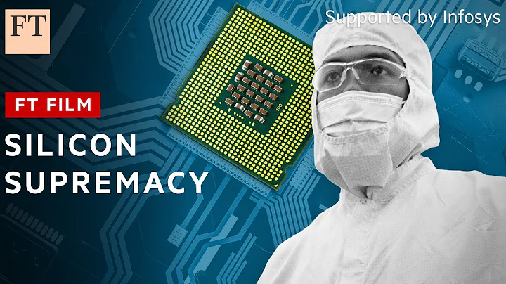
chip manufacturing
chip is the result of integrated circuit design, manufacturing, packaging and testing. From the manufacturing of raw material polysilicon to wafer , the key processes include silicon ingot casting, cutting, and cleaning. From monocrystalline silicon wafer to chip, it needs to go through photolithography, etching , ion implantation and other links. Finally, after packaging and testing, a ready-to-use chip is obtained.
Related companies in key processes
Wafer production: Transformation from gravel to silicon wafer
Ingot : First, the sand needs to be heated to separate the carbon monoxide and silicon, and the process is repeated until ultra-high purity electronic grade is obtained. Silicon (EG-Si). High-purity silicon melts into a liquid, and then solidifies into a single crystal solid form, called an "ingot". This is the first step in the manufacturing of semiconductors.
Cutting: Use a diamond saw to cut off both ends of the ingot, and then cut it into slices of a certain thickness. The diameter of the ingot sheet determines the size of the wafer. Larger and thinner wafers can be divided into more usable units, helping to reduce production costs.
Listed leading wafer foundry companies: SMIC, Wuhan Xinxin, and Hua Hong Semiconductor.
Lithography: Circuit printing that challenges the limits of physical precision
Lithography is to "print" circuit patterns onto wafers through light, which can be understood as drawing the planar diagram required for semiconductor manufacturing on the surface of the wafer. The higher the fineness of the circuit pattern, the higher the integration level of the finished chip, which must be achieved through advanced photolithography technology.
Through the irradiation of light, the components of photoresist undergo a chemical reaction to generate a circuit diagram. Limiting the minimum size that can be obtained by the finished product is directly related to the resolution that can be obtained by the lithography system, and reducing the wavelength of the irradiation light source is the most effective way to improve the resolution. Therefore, light source lithography machines have always been a research hotspot in various countries.
Domestic photolithography company: Hai Microelectronics Equipment Co., Ltd. (SMEE).
Etching: Removal of thin film waste on the surface of the wafer
After photolithography, the wafer needs to go through an etching process to remove the thin film layer that is not masked by the resist, so as to obtain the same pattern on the thin film as on the resist film. craftsmanship. To put it simply, etching is to use chemical, physical or both chemical and physical methods to selectively remove the part of the film layer that is not masked by the resist.
The two main types of etching are wet etching and dry etching . The etching process involving the use of liquid chemicals or etchants to remove the substrate material is called wet etching.
Listed etching equipment manufacturers: Micron Corporation , Northern Huachuang , Shengmei Shanghai, Yitang Semiconductor.
Ion implantation: Injecting fluidity into integrated circuits
Using a high-energy electric field to accelerate certain impurity ions at room temperature and then driving them into the surface of the wafer to change its physical, chemical or electrical properties. The energy of accelerated ions is usually a few to dozens of KeV, depending on how deep you want the ions to penetrate into the target. The higher the energy, the deeper the ions will be embedded. Another use of
high temperature is to allow the inserted atoms to replace the lattice positions occupied by the original silicon atoms. This can effectively release additional electrons or holes, greatly enhancing its conductivity.
Domestic ion implantation equipment manufacturer: Keshitong.
Lao Xie said
As the epidemic gradually stabilizes and semiconductor valuations return to rationality, companies in the key processes of chip manufacturing should have good investment opportunities.
Driven by rapidly developing emerging fields such as smart cars, 5G communications, artificial intelligence , and the Internet of Things, China's semiconductor chip industry will have a very fast market growth rate in recent years. China's semiconductor market has broad room for growth in the next few years.