SemiWiki reported that at the 2022 SPIE High-end Lithography Exposure Conference, ASML (ASML), a major extreme ultraviolet lithography equipment (EUV) manufacturer, introduced the latest progress of EUV. The outside world can understand the EUV development process and future development plans, which will have a profound impact on advanced semiconductors. Process development has a key influence.
ASML introduced that currently 0.33 EUV with aperture number is the main force in advanced semiconductor manufacturing processes. Both advanced logic and DRAM are produced using 0.33 EUV system. Taking a typical 5-nanometer process as an example, logic chips will be applied to more than 10 layers of EUV masks in 2021, and mass production of the 3-nanometer process will use 20-layer EUV masks in 2023. DRAM currently has about 5 layers of EUV masks, and soon it will DRAM uses approximately 8 layers of EUV masks. Partial exposure requires multiple images, and each chip may use up to 10 layers of masks.
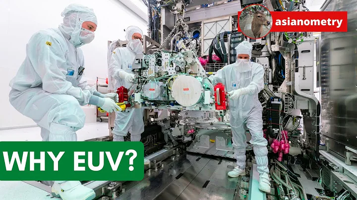
Logic chips and DRAM are gradually using EUV equipment. As of the first quarter, ASML shipped 136 EUV systems, exposing about 70 million chips. As the semiconductor manufacturing process increasingly requires EUV equipment, EUV innovation has been introduced and its reliability has also improved. ASML stated that the reliability of NXE:3400C is less than 90%, and the new generation NXE:3600D can reach 93%, which is close to the 95% reliability of deep ultraviolet exposure (DUV) lithography equipment. NXE:3600D can produce 160 chips per hour at a speed of 30mJ/cm², which is 18% higher than NXE:3400C. The NXE:3800E under development can initially reach 30mJ/cm², with a production capacity of approximately 195 chips per hour, and will eventually increase to 220 chips per hour.
It can be seen that in the field of EUV lithography exposure equipment with an ASML aperture number of 0.33, efforts are being made to improve production capacity and product power consumption. By 2025, the NXE:4000F will be launched with a production capacity of approximately 220 pieces per hour. ASML also continues to produce EUV production capacity and is expected to increase production capacity by 10% to 20%. It will deliver the first NXE:4000F exposure lithography equipment in 2025.
ASML is working hard to increase the production of EUV with an aperture number of 0.33, and is also developing the next generation of High-NA EUV exposure lithography equipment with an aperture number of 0.55. The data points out that it took about 10 years for the 0.33 High-NA EUV with an aperture number from the launch of the prototype in 2010 to the shipment of the mass production machine in 2019. Therefore, if the relevant reports are true, it means that the High-NA EUV equipment with an aperture number of 0.55 has shortened a lot of time from the launch of the prototype in 2023 to the shipment of the mass production machine in 2026, and it can be delivered to customers in only three years. Intel indicates the use of High-NA EUV equipment with an aperture number of 0.55 in 2025, and TSMC also announced the use of High-NA EUV equipment with an aperture number of 0.55 in 2026.
0.55 High-NA EUV optical components are much larger than 0.33 EUV and require unique design methods. The 0.55 High-NA EUV has an anamorphic lens system that has the same 4x reduction ratio as the 0.33 EUV in one direction and an 8x reduction ratio in the orthogonal direction. Due to the reticle size and 8x reduction ratio, the size of the exposed lithography area in the scanning direction can be halved to 16.5 nm.
In order to promote the use of 0.55 High-NA EUV faster, ASML has joined hands with many research institutions and companies, and Imec is an important partner. Imec CEO Luc Van den hove said that Imec cooperated with ASML to develop High-NA EUV technology, and ASML also developed the first EXE:5000 system prototype of 0.55 High-NA EUV. Compared with existing EUV systems, the EXE:5000 system can reduce the number of exposure and development times and complete the imaging of key features of logic chips below 2 nanometers.
In order to create an ecosystem of 0.55 High-NA EUV equipment, Imec continues to improve the projection resolution of 0.33 EUV lithography technology, predicts the imaging performance after the photoresist coating is thinned, and completes the reduction of line width, conductor spacing and contact precision pattern transfer wait. Imec also continues to work with material suppliers to demonstrate the test results of emerging photoresists and primer materials, hoping that the High-NA EUV process will have excellent imaging quality.
Imec also proposes new process-specific development and etching solutions to reduce lithographic image defects and random damage rates. As can be seen from the description, the 0.55 High-NA EUV needs to be updated not only in the exposure system, but also in the photomask, photoresist lamination and pattern transfer technology, etc., in order for the new equipment to be successfully mass-produced. Using 0.55 High-NA EUV requires upgrading not only the EUV system itself, but also photomask, photoresist and pattern transfer technology to make new equipment applications possible.
0.55 High-NA EUV is still in development, and Intel Mark Phillips has mentioned the possibility of 0.7 EUV becoming the successor to 0.55 EUV.Although ASML has ruled out the development of any new products after 0.55 High-NA EUV because ASML must invest heavily in EUV development, Mark Phillips pointed out that ASML has not completely ruled out the possibility of developing 0.7 or larger aperture number EUV systems and is still in the evaluation and research stage. .
Summary 0.55 EUV is the main system for advanced semiconductor manufacturing processes, and other systems are also improving reliability and productivity. As for 0.55 High-NA EUV, ASML is still developing it and will mass-produce it in 2025. It will have higher resolution and help simplify the procedures of advanced semiconductor manufacturing processes to reduce production costs. EUV with a higher aperture number is still being studied and will have the opportunity to be seen in production lines in 10 years.
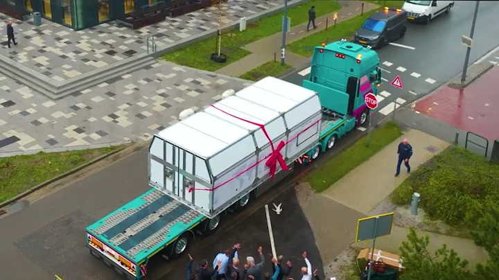
(first image source: ASML)