As we all know, the reason why TSMC has gained almost half of the world's share in the semiconductor (chip) foundry market is that it has excellent technology in semiconductor manufacturing processes. It currently leads the world in 7nm and 5nm, and the 3nm process R&D and mass production are also getting closer. Samsung Electronics is another giant that follows closely behind, and other semiconductor companies are slightly behind in this regard. Including and Intel , which have recently stated that they will return to the semiconductor foundry market, they have also suffered from process losses. They have been "skipping" their own advanced process production time, allowing companies such as AMD to grab a lot of share, and even Apple's latest research and development The computer chip M1 has also been mass-produced, and it is still manufactured by TSMC. When major partners no longer use Intel's chips, the pressure on them is understandable.
It can be said that advanced processes are extremely important for semiconductor manufacturing. The manufacturing process is actually a semiconductor process. What do 5nm, 7nm, 10nm, etc. represent? Ordinary users may not pay attention at all. However, we still often hear about the manufacturing process. In fact, to put it simply, the manufacturing process refers to the size of a chip that we can engrave one unit of transistor on. Chips produced by advanced processes are mainly used in mobile terminal products, such as mobile phones. Because the mobile phone processor is different from ordinary computer processors, the size left for the chip in the mobile phone is quite limited. The smaller the size, the more computing units there are in of the same size processor, and the stronger the performance. This is also the reason why manufacturers frequently emphasize the processor manufacturing process.
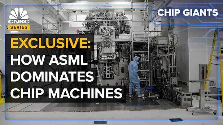
Another very important technical support is that as the frequency increases, the heat generated by the processor will also increase. Advanced etching technology can reduce the resistance between transistors and reduce the voltage required by the CPU, thereby reducing the power Significantly reduced. The benefit brought by the advanced process is that not only the performance is greatly improved, but the power consumption and heat generation are also continuously reduced. In terms of the layout of advanced processes, another equipment needs to be used, which is a new etching process - extreme ultraviolet lithography (EUV), which uses a smaller and sharper "knife" to cut out smaller transistor structures. This is why both TSMC and Samsung Electronics are rushing to buy the most advanced EUV lithography machine , and the gap between our companies in this regard is even greater.
Today, TSMC’s manufacturing process is ahead of other companies, and its technical capabilities are also the strongest. Including Samsung Electronics and Intel, there is a certain gap between them. Perhaps for this reason, Japanese officials will invest 42 billion yen to jointly develop the 2nm advanced process technology with Japan's three major semiconductor manufacturers - Canon , Tokyo Electron and Screen Semiconductor Solutions. At the same time, it will also establish a cooperative relationship with TSMC to seek to regain lost ground in the global semiconductor competition. In this market, TSMC and Samsung Electronics have plans.
Once upon a time, Japan was also a major semiconductor country. However, due to technological decline in recent years, it has been squeezed out of the forefront of the market. This time, Japan jointly manufactures photolithography machines, Canon, semiconductor manufacturer Tokyo Electronics, and semiconductor equipment manufacturer Screen Semiconductor Solutions to jointly develop 2nm advanced process technology. We also hope to make breakthroughs in advanced manufacturing technology. Moreover, as early as May 2020, news broke out repeatedly that the Japanese government invited foreign chip manufacturers to build wafer factories in Japan. However, TSMC later chose to build a factory in the United States.
It is reported that TSMC’s advanced packaging and testing plant will be located in Tokyo. Japan’s Ibaraki Prefecture Tsukuba City will also set up a new TSMC technology research and development center. The research and development content mainly involves wafer process research and development and 3D packaging. In the semiconductor manufacturing market, Japan actually has its own advantages. Among them, many Japanese manufacturers are involved in the EUV lithography process. For example, only Japanese manufacturers in the world can provide EUV photoresist .Five Japanese manufacturers, Tokyo Yinghua, Synthetic Rubber (JSR), Sumitomo Chemical , Shin-Etsu Chemical and Fujifilm , can produce EUV photoresist that is indispensable in the EUV lithography process. Japanese companies are very important in EUV lithography. The market share in the glue field is 100%.
At the same time, the EUV coating and development equipment produced by Tokyo Electronics can apply special chemical liquids to silicon wafers and develop them as semiconductor materials. In this field, Japanese companies are also unique. In addition to accumulating technology, Japanese semiconductor companies have also seen China's huge market demand and are actively deploying in the Chinese market. Among them, Ferrotec implemented capital increases and equity sales of its Chinese wafer subsidiary. After actively raising funds, we will invest in the mass production of 12-inch diameter wafer products used in cutting-edge semiconductors. Ferrotec has started mass production in Hangzhou, Zhejiang Province in 2020, and plans to increase production capacity to 100,000 pieces per month by 2022. The investment in expanding the wafer business is expected to reach at least 150 billion yen. For our companies, in terms of chip manufacturing, we should also dig deep into the market, invest technology research and development into mass production, and make up for the gap as soon as possible.