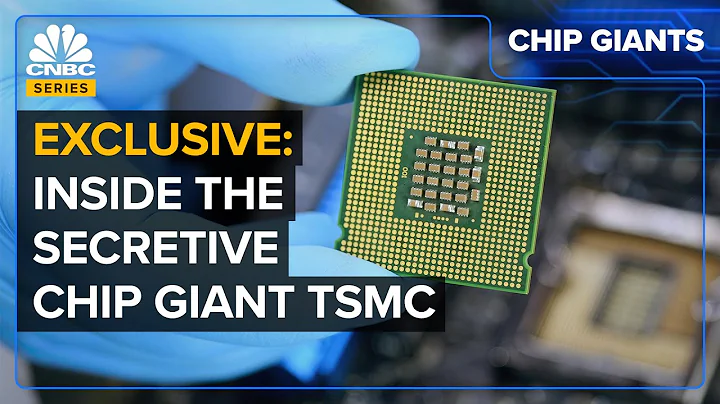
After the 10nm node, the only semiconductor manufacturing companies in the world that are capable of developing advanced processes are Intel , TSMC and Samsung. Among them, TSMC has the fastest progress in 7nm and later node processes and currently has almost a monopoly. 7nm chip foundry orders. TSMC's 5nm process will be trial-produced as soon as next year. After that, there will be a 3nm process. TSMC is still in the preparation stage. Yesterday, Taiwan's competent authorities passed the TSMC 3nm factory environmental difference plan. The total investment is expected to be no less than NT$600 billion. , which is a scale of US$20 billion, will start construction in 2020, and mass-produce 3nm technology by the end of 2022.

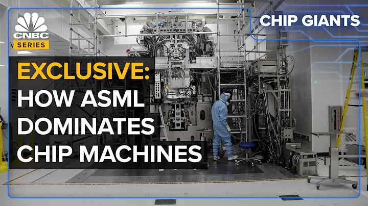
For 3nm wafer fabs, in addition to technology research and development, its consumption of water and electricity cannot be ignored, especially after the extensive use of EUV processes. We mentioned this issue before when introducing EUV lithography machines. Since EUV is extremely power-consuming, because 13.5nm ultraviolet light is easily absorbed, resulting in a very low conversion efficiency, which is said to be only 0.02%. The current output power of ASML's EUV lithography machine is 250W, which consumes 30,000 kilowatt hours of power for one day's work. The power consumption of wafer fabs is extremely alarming. The 2016 social responsibility report published by TSMC mentioned that the power consumption totaled 8.85 billion kilowatt-hours.
In addition to power consumption, wafer factories also require a large amount of water in the process of manufacturing chips. Large-scale wafer factories use up to 50,000 tons of water every day. Although more than 80% of water has been recycled, the total amount is still It’s amazing, so the construction of semiconductor wafer fabs still puts a lot of pressure on the environment. The more advanced the technology, the more obvious the problem becomes.
TSMC’s 3nm wafer fab is located in Taiwan’s Nanke Park, covering an area of 28 hectares, and is located close to TSMC’s 5nm fab. In mid-August this year, Taiwan's environmental protection department has passed the preliminary review of the " Tainan Science Park Phase II Base Development and Original Phase I Base Change Plan Environmental Deviation Case". Yesterday, the environmental difference case passed the review. TSMC will move from southern Taiwan in September 2020. After the Science and Technology Management Bureau obtained the land, it immediately started construction of a new 3-nanometer factory.
According to TSMC’s information, their 3nm project investment exceeds NT$600 billion, approximately US$19.4 billion or 134.7 billion yuan. Factory construction will begin in 2020, equipment installation will be completed in 2021, and mass production is expected from the end of 2022 to early 2023.


