Yesterday Samsung Electronics announced that it has begun mass production of chips based on 3nm GAA (Gate-all-around) process technology technology. This also makes Samsung take the lead in TSMC and become the first in the world. Mass production of 3nm wafer foundry company . According to Bloomberg, Samsung has begun producing 3-nanometer chips, beating rival TSMC to adopt a more power-efficient manufacturing process. Currently, there are three manufacturers in the world that are willing and able to develop 3nm chip manufacturing: TSMC, Samsung, and Intel . According to the plan, TSMC's 3nm process will be mass-produced in the second half of 2022, and Intel 4, which is renamed from Intel's 7nm process, is also scheduled to be mass-produced in the second half of 2022.

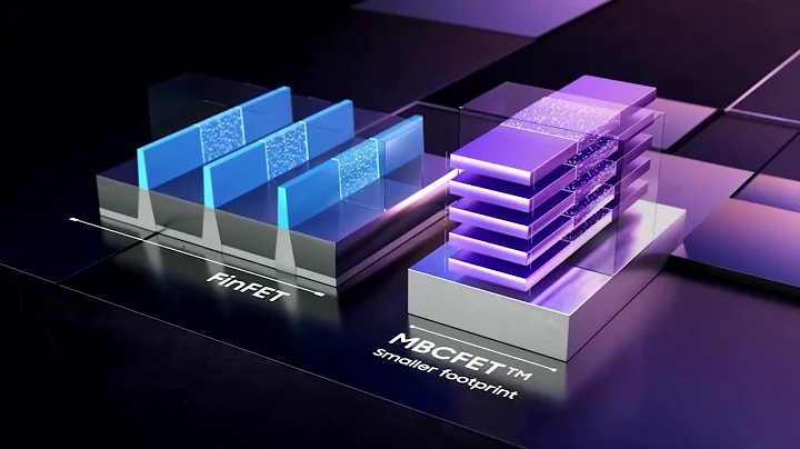
According to data released by Samsung, compared with the 5nm process, the 3nm process can reduce power consumption by 45%, improve performance by 23%, and reduce chip area by 16%. In the future, it hopes its second-generation 3nm process will reduce power consumption and size by 50% and 35% respectively, and improve performance by 30%. In addition to being the first to mass-produce 3nm process technology, Samsung is also the first wafer foundry in the world to successfully apply GAA technology to mass-produced 3nm chips. The commissioning of the
factory also broke a lot of suspicion in the industry. Previously, the Taiwanese industry believed that Samsung might have to postpone mass production because of the low yield rate of 3nm. Objectively speaking, this suspicion has a historical basis. Samsung has been working hard to catch up with TSMC's advanced processes, but the pace is too big and the yield rate has become a hidden danger from time to time. In the wafer foundry market, Samsung also lags behind TSMC's share.
TSMC said it would not comment on Samsung’s breakthrough progress. It is said that TSMC’s 3nm process based on FinFET architecture will enter the mass production stage and be paired with FINLEX architecture. In addition, the 2nm process is expected to be mass produced in 2025. The announcement is a key milestone in Samsung's efforts to compete with TSMC, which dominates the contract chip production market and is the maker of chips used by Apple Inc. for its iPhones, iPads, MacBooks and Macs.
In fact, Samsung has been dominated by TSMC in the field of chip manufacturing. But last year, Samsung announced an investment plan of 171 trillion won (approximately 884.07 billion yuan). It is expected to surpass TSMC to become the world's top logic chip manufacturer by 2030, and will find new opportunities in China in its foundry business. client! It is also said that TSMC's 3nm process is expected to enter production later this year. The chips will initially be produced for "high-performance, low-power computing" applications, but it plans to eventually use them in the mobile field.