Samsung has begun mass-producing chips using its 3nm process node, its most advanced chip production technology that allows smaller chips to pack more power.

Samsung said on Thursday it has begun mass production of chips using its 3-nanometer (nm) process node, its most advanced technology yet for contract chip production.
The South Korean tech giant said its 3nm process reduces power consumption by 45%, improves performance by 23% and reduces surface area by 16% compared to the 5nm process.
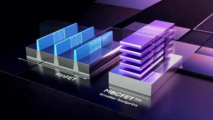
Samsung ’s 3nm process node uses its Gate All-Around (GAA) transistor architecture, which the company calls Multi-Bridge Channel FET (MBCFET), which packs wider channels into the gate for current flow, while being compatible with previous FinFET transistor architecture reduces voltage levels compared to
As the name GAA implies, the channel is completely surrounded by the gate, and utilizing all four sides of the channel allows more drive current to pass through the gate than a FinFET using only three sides.
The South Korean tech giant also touts that its 3nm process node offers flexible designs, allowing it to adjust channel widths to best meet customer needs. Samsung said that the subsequent second-generation 3nm process node is also under development, with improvements in power consumption, performance and surface area.
Samsung said that the chips currently manufactured through its first 3nm process node are used in high-performance, low-power computing applications, while it plans to expand this node to mobile processors. The South Korean tech giant did not mention which customer it is currently mass producing 3nm chips for.
Samsung is the world's largest memory chip maker and the second-largest contract chipmaker, or foundry. It is competing with Taiwan Semiconductor Manufacturing Co., Ltd. (TSMC), the world's largest foundry, which is preparing to start mass production using its own 3nm process node, commercializing more advanced process nodes first.
The key to the love-hate relationship between this "couple" is how to win more orders from other customers for their respective 3nm chips, rather than more orders from big customers such as Qualcomm .
Last month, Samsung announced plans to spend $355 billion over the next five years on so-called strategic businesses, which include semiconductors. Last year, the company announced it would spend $17 billion to build a new chip factory in Tyler, Texas.