The laboratory of leading Intel (Intel) recently announced that it has made significant progress in integrated photonic research. This will be the next technological frontier to improve the bandwidth between data center computing chips and the overall network communication. The latest research shows that using multi-wavelength integrated optics to provide an 8-wavelength distributed feedback (DFB) laser array fully integrated into the silicon chip can provide very good ±0.25 decibel (dB) output power uniformity and exceed industry specifications. ±6.5% wavelength spacing uniformity.
According to Rong Haisheng, senior technical director of Intel Labs, this new research shows the possibility of achieving good matching output power, as well as uniform and high-density wavelength spacing. More importantly, it can be accomplished through the existing manufacturing and process control of Intel chip fabs, providing a clear direction for next-generation mass production machine manufacturing of co-packaged optics and optical computing interconnects. Additionally, this advancement enables the creation of light sources with the performance required for a host of future applications, such as co-packaged optics and optical computing interconnects for emerging network-intensive workloads such as artificial intelligence (AI) and machine learning (ML). The laser array is manufactured using Intel's 12-inch silicon photonics process and is ready for future mass production machine manufacturing and widespread deployment.
Intel said that Gartner estimates that the proportion of silicon photonics occupying all high-bandwidth data center communication channels will increase from less than 5% in 2020 to more than 20% in 2025, with the overall potential market size reaching US$2.6 billion. The growing need for low power consumption, high bandwidth and higher speed data transmission is driving the demand for silicon photonics to support data centers and other further applications.
In fact, optical connections began to replace copper wires in the 1980s because of the inherent properties of optical transmission through fiber providing high bandwidth, unlike the transmission of electrical pulses through metal wires. Since then, as component size and cost have decreased, the technology has become more efficient, leading to a breakthrough in networking solutions using optical interconnects over the past few years. Generally speaking, this has happened with switches. , data centers and other high-performance computing environments. As electrical interconnection performance limits are gradually approached, integrating closely adjacent chip circuits and optical components in the same package can improve energy efficiency while completing longer connection distances, ensuring the future of input/output (I/O) interfaces. These photonic technologies are completed through existing process technologies in Intel factories and enjoy the advantage of large-scale manufacturing that helps reduce costs.
Intel also emphasized that recent co-packaged optical solutions using high-density wavelength division multiplexing (DWDM) technology have proven that while increasing bandwidth, they can also significantly reduce the physical size of optical chips. However, until now, it has been difficult to manufacture DWDM light sources with uniform wavelength spacing and power consumption. Therefore, Intel's new breakthrough ensures that the light source has consistent wavelength separation and maintains uniform output power, thus meeting one of the requirements for optical computing interconnection and DWDM communications. Next-generation computing I/O using optical interconnects can be tailored for the extreme demands of future high-bandwidth AI and ML workloads.
Intel further emphasized that this 8-wavelength DFB array is designed and manufactured using Intel's commercial 12-inch hybrid silicon photonics platform, which is also used to manufacture mass-produced optical transceivers. This innovation is a major advance in the laser manufacturing capabilities of a fab that mass-produces complementary metal oxide semiconductors (CMOS) and uses the same lithography technology and strict process controls used to make 12-inch silicon chips.
In addition, in this research, Intel used advanced lithography technology to define waveguide gratings in silicon before the Group 3 and 5 chip bonding process. Compared with traditional semiconductor lasers manufactured in 3-inch or 4-inch III-V chip factories, this technology achieves better wavelength uniformity. In addition, due to the tight integration of the lasers, the array is able to maintain its channel spacing as the ambient temperature changes.
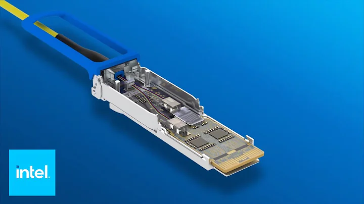
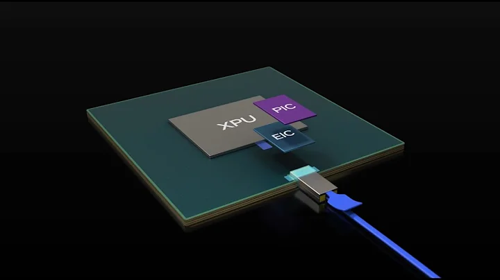
Intel finally stated that it is committed to developing solutions to meet the growing needs for higher efficiency and richer resources in network infrastructure. The core technology components under development include light generation, amplification, detection, modulation, CMOS interface circuits, and packaging integration technology. Additionally, many aspects of the 8-wavelength integrated laser array technology are being implemented by Intel's Silicon Photonics Group as part of future optical computing interconnect chiplets. Upcoming products provide energy-efficient, high-performance multi-Tb/s interconnects between various computing resources such as CPU, GPU and memory. Integrated laser arrays are a compact and cost-effective solution that is indispensable in supporting the manufacturing and deployment of high-volume production machines.
(first image source: provided by Intel)