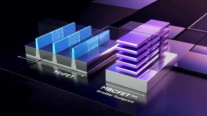
Samsung (Samsung) announced the mass production of 3 nanometer GAA technology. Industry experts said that the global GAA ecosystem is not yet fully in place. The mass production of Samsung's 3 nanometer GAA technology is just a rush to put it on the shelves. It should only be used by itself at present, and there are no external customers. Samsung is actively competing for the wafer foundry market. In order to overtake its archrival TSMC, it decided to adopt the surround gate (GAA) architecture in 3nm, and in the first half of the year before TSMC’s 3nm mass production in the second half of the year. On the last day, mass production of 3nm GAA technology was announced. TSMC had no comment. South Korean semiconductor analyst Greg Roh was recently interviewed and viewed the progress of Samsung's 3-nanometer process positively, saying that Samsung's 3-nanometer process yield rate improvement is much faster than market expectations, and the speed of adding customers is quite fast. South Korean media reported that Chinese mining machine chip designer Shanghai Pansilicon Semiconductor is a customer of Samsung's 3-nanometer process. In addition, the US chip factory Qualcomm (Qualcomm) has also ordered Samsung's 3-nanometer production capacity, but it will be put into production depending on the situation. . Yang Ruilin, research director of the International Institute of Obstetrics and Mechanics of the Industrial Research Institute, held a different view. He pointed out that ASML ( ASML ) is the first high numerical aperture extreme ultraviolet (high-NA) device produced by Belgian Microelectronics Research Center (Imec). EUV) lithography exposure equipment is expected to be completed and used for research and development in 2023. It is speculated that mass production of Samsung's 3-nanometer GAA technology does not use high-NA EUV lithography exposure equipment. In addition, GAA-related etching and measurement problems have yet to be overcome, and materials, chemicals, etc. also need to be improved. Yang Ruilin said that the global GAA ecosystem is not yet fully in place, and mass production of Samsung's 3-nanometer GAA technology at this time is "rushing the ducks to the shelves." ”. Yang Ruilin said that if Samsung adopts the existing solutions in the market, it is not that it cannot mass-produce 3-nanometer GAA technology. The key is that the cost will increase, the delivery time will be lengthened, the yield rate will be slow, and the quality will not necessarily be good. Since it is difficult to establish a cost model, it is difficult for Samsung to quote prices to customers. It is expected that Samsung's 3-nanometer GAA technology will only be used by itself and will not have external customers. Liu Peizhen, researcher and director of the Industrial Economics Database of the National Taiwan Institute of Economics, also said that Samsung has not actually received 3 nanometer orders. Today’s announcement of mass production of the 3 nanometer process should have more publicity than substantive significance. Domestic legal persons pointed out that Samsung has always used low-price strategies to attract customers. Cheap quotes may be able to win orders from Shanghai Pansilicon Semiconductor. However, heat dissipation is a pain point for Samsung, and Qualcomm orders are therefore returned to TSMC; Can Samsung's 3nm GAA process solve the problem of leakage, Thermal issues remain to be seen. Yang Ruilin believes that TSMC’s advanced process development schedule is relatively reasonable and gradual. TSMC’s 3nm will be mass-produced in the second half of this year. With the innovative FINFLEX architecture, it will provide chip designers with diverse choices, including support for ultra-high performance and optimal power consumption efficiency. With transistors density and balance the high performance of both. Mi Yujie, senior vice president of research and development at TSMC, recently stated at the North American Technology Forum that TSMC will obtain high-NA EUV exposure equipment in 2024 in response to customers' needs to promote innovation. Yang Ruilin said that by then the GAA technology-related ecosystem will become more complete, and TSMC’s 2-nanometer process using nanosheet transistor architecture will begin mass production in 2025. It is expected that TSMC will still maintain its leading position in advanced process technology. Liu Peizhen said that TSMC’s 3-nanometer process has already mastered orders from Apple (Apple), Intel ( Intel ) and other heavyweight customers. Obviously, customers are more interested in TSMC’s 3-nanometer process yield, mass production stability and output. Confidence, believing that TSMC will continue to lead the world in advanced manufacturing processes.


