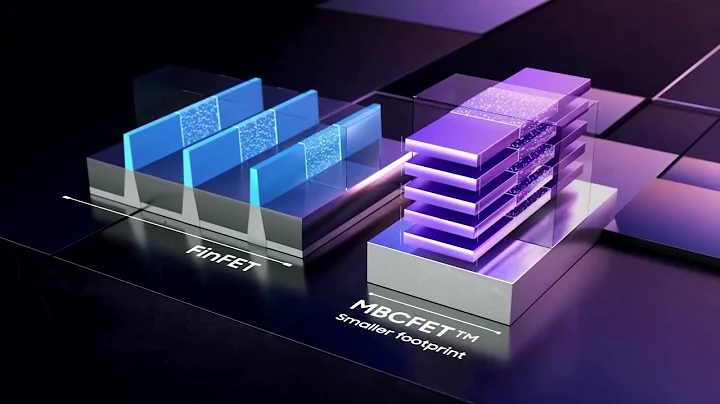
According to Korean media reports, Samsung Electronics today officially put into production the 3nm process chip manufacturing of the GAA architecture, laying the foundation for catching up with TSMC. According to reports, the GAA architecture is superior to the currently widely used FinFET architecture.
TSMC has previously announced that it will mass produce the 3nm process in the second half of this year. This means that Samsung has overtaken TSMC at the advanced process level for the first time. In addition, Intel is expected to mass-produce 3nm process chips in the second half of next year. The commissioning of the

factory also broke a lot of suspicion in the industry. Previously, the Taiwanese industry believed that Samsung might have to postpone mass production because of the low yield rate of 3nm.
Objectively speaking, this suspicion has a historical basis. Samsung has been working hard to catch up with TSMC's advanced processes, but the pace is too big and the yield rate has become a hidden danger from time to time. In the wafer foundry market, Samsung also lags behind TSMC's share.
TSMC said it would not comment on Samsung’s breakthrough progress. It is said that TSMC’s 3nm process based on FinFET architecture will enter the mass production stage and be paired with FINLEX architecture. In addition, the 2nm process is expected to be mass produced in 2025. According to
data, 60% of Samsung’s chip manufacturing capacity is supplied to the group’s companies. It is expected that this 3nm production capacity will be no exception and will be used first by Samsung Group .
C114 Communication Network Nanshan