Recently, the news that Korean semiconductor manufacturer Samsung has taken the lead in wafer leading foundry TSMC and mass-produced 3 nanometers has attracted great attention in the industry. The latest news is that Samsung has officially announced the mass production of 3nm chips.
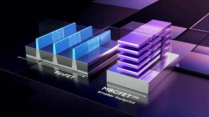
Today (June 30), Samsung announced through its WeChat public account "Samsung Semiconductor and Display Official" that chips based on the 3nm all-around gate (Gate-All-AroundT, referred to as GAA) process technology node have begun preliminary Production, first of all, will be used in the field of high-performance, low-power computing semiconductor chip , and plans to expand it to the field of mobile processors.
Compared with Samsung's 5nm process, Samsung's first-generation 3nm process can reduce power consumption by 45%, improve performance by 23%, and reduce chip area by 16%; Samsung said that in the future, the second-generation 3nm process will reduce power consumption by 50%. The performance is improved by 30% and the chip area is reduced by 35%.
As for 3-nanometer customers, media reports said that sources revealed that Samsung said it had customers ordering production capacity, including virtual currency mining machine chip design company Shanghai PanSemi, and mobile processor major Qualcomm (Qualcomm), etc., but Qualcomm will conduct production depending on the situation.
Judging from the time point, Samsung’s 3-nanometer technology mass production time is indeed ahead of TSMC.

According to the process technology development blueprint and future plans shared by TSMC at a recent technical seminar in North America, its initial 3-nanometer node (N3) is expected to begin mass production in the second half of this year and be delivered to customers early next year. In addition, TSMC will also launch a variety of N3 derivative manufacturing processes in the next few years. In terms of
2nm process technology, TSMC revealed that the N2 process node will use the GAAFET architecture for the first time and is planned to be put into production in 2025.
Source of article: Compiled by Global Semiconductor Observation Niki