
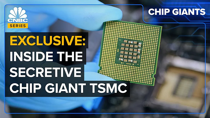
TSMC’s booth at the 2021 World Semiconductor Conference (Photo source: Titanium Media App editor)
The long-rumored 2nm is finally here.
According to news on June 17, Titanium Media App learned that at the TSMC North American Technology Forum held early this morning, TSMC (TSMC) officially announced its future advanced process roadmap.
Among them, TSMC's 3nm (N3) process will be mass-produced in 2022, and TSMC will launch the 2nm (N2) process technology using the nanosheet transistor (GAAFET) architecture for the first time, which will be mass-produced in 2025.
TSMC President Wei Zhejia said at the online forum that in a rapidly changing and rapidly growing digital world, the demand for computing power and energy efficiency is increasing faster than ever before, opening up unprecedented opportunities and challenges for the semiconductor industry. At this exciting time of transformation and growth, the innovations revealed by TSMC at the technology forum demonstrate TSMC’s technology leadership and commitment to supporting customers.
At the same time, TSMC senior vice president of R&D YJ Mii announced at this meeting that TSMC will have the most advanced and latest high numerical aperture extreme ultraviolet (high) lithography machine giant ASML in 2024. -NA EUV) exposure machine lithography equipment, the second generation EUV lithography machine. "Mainly used for partners' research purposes... to develop solutions related to infrastructure and formats based on customer needs and promote innovation."
TSMC manufacturing process roadmap, 2nm will begin mass production in 2025
Specifically Said that the core of this TSMC Technology Summit is to announce the specific technical details of the leading nodes of the N3 (3nm level) and N2 (2nm level) series, as well as the TSMC-3DFabricTM three-dimensional silicon stacking solution, which will be used in manufacturing in the next few years. Advanced CPU, GPU and mobile SoC chip products.
- 3nm technology node: TSMC’s first 3nm-level node is called N3. It is expected to start high-volume manufacturing (HVM) mass production in the second half of this year and is expected to be delivered to customers in early 2023. Among them, the 3nm second node N3E, compared with N5, at the same speed and complexity, N3E reduces power consumption by 34%, improves performance by 18%, and increases logic transistor density by 1.6 times, and with the advanced TSMC FinFlextm architecture, it can Accurately assist customers in completing system-on-chip designs that meet their needs.
- 2nm technology node: TSMC’s first 2nm node is called N2, which uses a nanosheet transistor (GAAFET) architecture and is expected to start mass production in 2025. It is reported that under the same power consumption, the performance speed of 2nm is 10% to 15% faster than that of 3nm. At the same speed, the power consumption is reduced by 25% to 30%. TSMC also stated that the 2nm process technology platform also covers high-performance versions and complete chiplet integration solutions.
- expands ultra-low power platform: TSMC said it is developing N6e technology, focusing on edge artificial intelligence and Internet of Things devices. N6e will be based on the 7nm process, and its logic density is expected to be three times higher than that of the previous generation N12e. It is reported that the N6e platform covers logic, radio frequency, analog, embedded non-volatile memory, and power management IC solutions.
- TSMC-3DFabricTM three-dimensional silicon stacking solution: TSMC demonstrated two breakthrough innovations today. One is a SoIC-based CPU that uses chip stacking on wafer (Chip-on-Wafer, CoW) technology. Stacked three-level cache static random access memory; the other is an innovative AI SoC that uses Wafer-on-Wafer (WoW) technology to stack on deep trench capacitor chips.
TSMC stated that 7nm chips equipped with CoW and WoW technologies are currently in mass production, and 5nm technology is expected to be completed in 2023. In order to meet customer needs for system integration chips and other 3D Fabric system integration services, the first fully automated 3D Fabric wafer fab is expected to start production in the second half of 2022.
As TSMC 2nm shifts to the nanosheet-based GAAFET architecture, the 3nm series will become the last technology platform for TSMC’s FinFET node. It is expected that after mass production of 2nm chips in 2025, TSMC will continue to produce 3nm semiconductor products.
In addition, TSMC revealed that its mature and professional node production capacity will expand by approximately 50% by 2025.The plan includes the construction of a large number of new wafer fabs in Tainan, Kaohsiung, Japan and Nanjing. This move will further intensify the relationship between TSMC and wafer foundries such as GlobalFoundries, UMC and SMIC. competition between.
According to AnandTech reports, the four new facilities for expansion of mature and professional node investments are: TSMC’s Fab 23 Phase 1 plant in Kumamoto, Japan, manufactures 12nm, 16nm, 22nm and 28nm chips, and will have up to 45,000 300 pieces per month Millimeter (12-inch) wafer production capacity; Tainan Fab 14 Phase 8; Kaohsiung Fab 22 Phase 2; Nanjing Fab 16 Phase 1B, currently mainly produces 28nm mature process chips.
Currently, TSMC has 13 wafer foundries around the world. Among them, 10 factories are located in Taiwan, China, 2 are in Shanghai and Nanjing, manufacturing 8-inch and 12-inch wafers respectively; 1 is in Fab11 in the United States, manufacturing 8-inch wafers. TSMC's 7nm and 5nm advanced process chips are mainly produced at the Tainan Fab18 factory.
(This article was first published on Titanium Media App, author | Lin Zhijia)


![【未播】不想做蛋糕师的歌手不是好Jolin《王牌对王牌2》第4期 20170210 [浙江卫视官方HD] 王源 王祖蓝 宋茜 - DayDayNews](https://i.ytimg.com/vi/_rVld7gMCG8/hq720.jpg?sqp=-oaymwEcCNAFEJQDSFXyq4qpAw4IARUAAIhCGAFwAcABBg==&rs=AOn4CLD5U3yH6ElXqEIyyqUg6gPNRFMCmg)


![浙江卫视春晚:跑男团惊喜亮相 babyLucas首合唱 《浙江春晚》 花絮 ALL FOR RUN [浙江卫视官方HD] - DayDayNews](https://i.ytimg.com/vi/W87oUORp9p0/hq720.jpg?sqp=-oaymwEcCNAFEJQDSFXyq4qpAw4IARUAAIhCGAFwAcABBg==&rs=AOn4CLDlGC2MqBGgWT6-nTOw-gJdi_JazQ)


![【4/6】SING!CHINA EP.3 Sneak Peek 20160729 [ZhejiangTV HD1080P] - DayDayNews](https://i.ytimg.com/vi/9KuekAr2DzA/hq720.jpg?sqp=-oaymwEcCNAFEJQDSFXyq4qpAw4IARUAAIhCGAFwAcABBg==&rs=AOn4CLBQ8NeKw_h2-S8jTAohutPNdeB8Xw)
