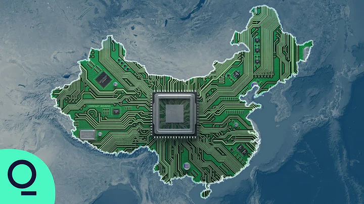
Although breakthroughs in chip manufacturing processes below 10 nm have become increasingly difficult, industry leading companies represented by TSMC have not slowed down the pace of research and development. The company said last week that development of its 3nm process is progressing well. At present, it seems that TSMC has figured out the path and has begun to contact early customers. TSMC CEO and co-chairman CC Wei made the announcement during a conference call with investors and financial analysts.

He said: "Our company is making good progress in the technology development of the N3 node, and has been in contact with early customers on technology definition. We hope that the 3nm process can further increase TSMC's industry leadership in the future."
Because N3 technology is still in the early development stage, TSMC has not yet talked about specific features and its advantages over N5. The company said it has evaluated all possible transistor structure options and provided customers with a very good solution. The N3 specification is under development and TSMC believes it will meet the requirements of its industry-leading partner customers. In fact, TSMC has confirmed that N3 will be an entirely new process, rather than a simple improvement or iteration of N5.
Samsung, one of the company's main competitors, plans to use 3nm technology. At the same time, it is certain that TSMC’s 3nm node will use both deep ultraviolet and extreme ultraviolet lithography equipment. Since TSMC's N5 process uses 14 layers of EUV, N3 may use a higher number of layers. As the world's largest semiconductor contract manufacturer, it seems very satisfied with the progress of EUV and believes that the technology is crucial to its future development.
Editor’s comment: The advancement of 3 nanometers has allowed TSMC to enter the frontier market earlier. What is certain is that the 3 nanometer chips do not adopt the old version of the design ideas, and have greater improvements in technology and manufacturing processes, using more layers. , it is foreseeable that TSMC will have a greater say in the 3-nanometer chip field in the future.
[ZOL client download] To view the latest technology information, search "ZOL Online" in the APP market, and the client reading experience will be better. (7226451)