Samsung mass-produces the 3nm GAA process, and Haipan Silicon is the first customer
In June 2021, Samsung was the first to announce that its 3nm process based on GAA technology has been successfully taped out. Subsequently, at the "Samsung Foundry Forum 2021" event of in October 2021, Samsung announced that it would take the lead in producing 3nm GAA process technology from TSMC in the first half of 2022.
Samsung is also full of confidence in surpassing TSMC in 3nm mass production. Jeong Eun-seung, the technical head of Samsung Device Solution Division, said last year, "Samsung only established the wafer foundry division in 2017, but with the company's expertise in storage manufacturing, it is just around the corner to surpass TSMC." He also For example, Samsung once led TSMC in launching mass production of the 14nm process using FinFET technology.
Although there have been many rumors in the industry about Samsung's 3nm yield rate being too low, which has caused difficulties in mass production (early this year, it was revealed that the yield rate of Samsung's 3nm GAA process is only 10%~20%), but Samsung is still in 2022 On the last day of the first half of the year (June 30), it officially announced the successful mass production of the 3nm GAA process to fulfill its previous commitments.
According to Samsung’s official statement, compared with traditional 5nm process chips, chips based on its first-generation 3nm GAA process reduce power consumption by 45%, improve performance by 23%, and reduce area by 16%.
However, the above published data has shrunk to a certain extent from the data previously disclosed by Samsung ( performance will be improved by 30%, energy consumption can be reduced by 50%, and logical area efficiency will be improved by more than 45% ).
It should be emphasized that in addition to being the first to mass-produce the 3nm process technology, Samsung is also the first wafer foundry in the world to successfully apply GAA technology to mass-produced 3nm chips. Although TSMC will mass-produce it in the second half of this year, It produces 3nm process, but it is still based on FinFET transistor architecture. TSMC will use GAA technology on 2nm process technology, and the mass production time will be in 2025.
Siyoung Choi, head of Samsung's foundry business, said: "The company will continue to actively innovate in competitive technology development."
Chinese mining chip manufacturer Shanghai Pansi may be the first customer
Although Samsung has not announced its 3nm There is a list of customers for the GAA process, but according to the news, Samsung Electronics itself and a mining chip manufacturer from mainland China - Shanghai Pan Silicon Semiconductor Technology Co., Ltd. will be the first customers. In addition, Samsung's major customer Qualcomm may also place an order to produce 3nm chips, but it will be put into production depending on the situation.
According to data, Shanghai Pan Silicon Semiconductor Technology Co., Ltd. was established in March 2016 with a registered capital of 45 million yuan. is headquartered in Shanghai. It is a high-tech start-up company with design capabilities for 28nm, 16nm and 10nm ASIC, focusing on digital ASIC design for cryptocurrency and AI applications.
Samsung co-chief executive Kyung Kye-hyun said earlier this year that its foundry business would seek new customers in China, where it expects rapid growth as companies from automakers to home appliance makers compete. to ensure production capacity to address the ongoing global chip shortage.Is
"real mass production" or "real propaganda"?
Although Samsung produced the 3nm GAA process technology ahead of TSMC, in order to fulfill its mass production commitment in the first half of this year, it only announced mass production on June 30, the last day of the first half of the year, which also led some analysts to believe that its 3nm GAA process technology Mass production of technology is "rushing ducks to the shelves", and the promotional significance is greater than the actual significance.
For example, Yang Ruilin, the research director of the Institute of Obstetrics and Technology, Taiwan Industrial Research Institute, said that GAA-related etching and measurement problems have yet to be overcome, and materials, chemicals, etc. also need to be improved. The global GAA ecosystem is not yet fully in place. Samsung’s 3nm GAA technology has not yet been fully developed. Mass production is a matter of "rushing the ducks to the shelves".
ASML's new generation High-NA EUV lithography machine is expected to be delivered to customers as early as the end of 2023. Both TSMC and Intel have chosen to use the High-NA EUV lithography machine to produce 2nm processes based on GGA architecture transistors.
Yang Ruilin said that although Samsung can achieve mass production of 3nm GAA technology using existing solutions in the market, the key is that the cost will increase, the delivery time will be lengthened, the yield rate will increase slowly, and the quality is not necessarily good. Since it is difficult to establish a cost model, it is difficult for Samsung to quote prices to customers. It is expected that Samsung's 3nm GAA technology will only be used by itself and there will be no real external customers.
Liu Peizhen, researcher and director of the Industrial Economics Database of the National Taiwan Institute of Economics, also said that Samsung has not actually received 3nm orders yet. Today’s announcement of mass production of the 3nm process should be more publicity than substantive.
Prior to this, Samsung's process technology performance in terms of stability, yield, heat generation, etc. has always been worse than TSMC's at the same process node. Previously, Qualcomm switched to using TSMC's 4nm OEM Snapdragon 8+ due to heat dissipation issues with Samsung's 4nm OEM Snapdragon 8.
However, the stance and opinions of Taiwan’s relevant institutions are often biased towards local TSMC, and it is normal to be negative about Samsung’s 3nm GAA.
Similarly, South Korean semiconductor analysts are often optimistic about local Samsung. Previously, South Korean semiconductor analyst Greg Roh said that Samsung’s 3nm process yield rate increased much faster than market expectations, and the rate of new customers was quite fast. What are the advantages of
GAA architecture transistors?
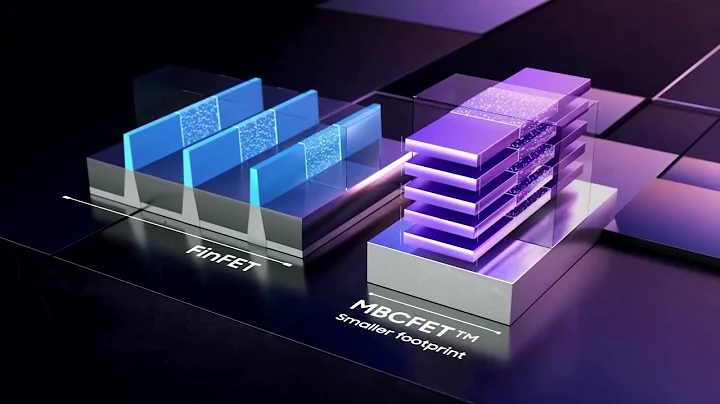
Traditional planar transistors (Planar FET) save power consumption by reducing voltage. However, the short channel effect of planar transistors limits the continued reduction of voltage, and the emergence of FinFET ( Fin Field Effect Transistor ) allows the voltage to be restored again Reduced, but as the process continues to advance, FinFET is no longer enough to meet demand. As a result, GAA (Gate-all-around) technology came into being.
As shown below, the typical GAA form - GAAFET (Gate-all-around FETs) uses a nanowire channel design. The entire outer contour of the channel is completely wrapped by the gate, which represents the gate's control over the channel. better. In contrast, the traditional FinFET channel is surrounded by gates on only 3 sides. The transistor of the GAAFET architecture provides better electrostatic characteristics than FinFET and can meet certain gate width requirements. This is mainly reflected in the enhanced channel control capability of GAA under the same size structure, and the size can be further reduced.
However, Samsung believes that the use of nanowire channel design is not only complicated, but also the cost may be greater than the benefits. Therefore, Samsung designed a new form of GAA - MBCFET (Multi-Bridge-Channel FET, multi-bridge-channel field effect transistor), using multi-layer stacked nanosheets to replace the nanowires in GAAFET. This nanosheet design has been extensively studied by the research institute IMEC as a follow-up product to the FinFET architecture, and was developed by IBM in cooperation with Samsung and GlobalFoundries.
Samsung said that MBCFET can minimize complexity while retaining all the advantages of GAAFET.At the same time, the design of MBCFET is compatible with previous FinFET technology, and the design of FinFET can be directly migrated to MBCFET, improving performance without increasing the area.
In addition, in the manufacturing process, this technology is also highly manufacturable because it utilizes about 90% of FinFET manufacturing technology and equipment and only requires a small amount of modified masks.
Samsung stated last year that MBCFET’s excellent gate controllability is 31% higher than Samsung’s original FinFET technology, and the nanosheet channel width can be directly changed graphically, making the design more flexible.
Samsung's 3nm GAA (MBCFET) process is divided into two stages: 3GAAE (3nm Gate-AlI-Around Early) and 3GAAP (3nm Gate-AlI-Around Plus). Currently in mass production is 3GAAE.
It should be pointed out that Samsung’s 3nm process based on GAA technology is different from TSMC’s FinFET architecture 3nm process. Therefore, if Samsung wants to successfully mass-produce the 3nm GAA process, it also needs new design and certification tools.
It is understood that Samsung’s 3nm GAA process technology uses the Fusion Design Platform of Synopsys to provide a highly optimized reference method for its GAA architecture production process. The physical design kit (PDK) for Samsung's 3nm GAA process technology was released as early as May 2019 and passed the process technology certification in 2020.
Shankar Krishnamoorthy, general manager of Synopsys' digital design department, said at the time that the GAA transistor structure symbolizes a key transition point in the progress of process technology and is crucial to maintaining the strategies required for the next wave of ultra-large-scale innovation. Synopsys' strategic partnership with Samsung supports the provision of best-in-class technologies and solutions, ensuring the continuation of development trends and providing opportunities for the semiconductor industry.
TSMC and Intel will introduce GAA technology in 2nm
In order to catch up with TSMC, Samsung has been relatively aggressive in advancing advanced processes. In contrast, TSMC, the industry leader, has always been relatively stable.
TSMC did not choose GAA architecture transistors in the 3nm process technology, but still used FinFET (Fin Field Effect Transistor), because this will bring better stability to TSMC, that is, it can reuse previously mature and stable ones. technology, while costs may also be better controlled. And give TSMC more time to optimize the GAA transistor architecture.
According to data previously released by TSMC at 2022 TSMC Technology Forum, its upcoming mass production still uses the FinFET transistor architecture N3E (a low-cost version of 3nm) process technology. Compared with the previous generation 5mm process technology, the performance will be lower. Increased by 18%, power consumption can be reduced by 34%, and transistor density can be increased by 30%.
Judging from this data, the performance improvement and power consumption reduction brought by Samsung's 3nm GAA process technology compared with its previous generation 5nm process technology are higher than those of TSMC (3nm VS. 5nm).
Moreover, it should be pointed out that the transistor density of Samsung's 3nm GAA process is only 16% higher than the transistor density of its predecessor process ( area can be reduced by 16%). The transistor density of TSMC’s 3nm is 30% higher than that of its 5nm. means that Samsung 3nm GAA manufacturing process process technology relies on less improvements in transistor density to achieve better performance improvements and power consumption reductions. Obviously, this is consistent with the improvements brought about by the new GAA architecture. D.
Our can also see the direct improvement brought by the GAA transistor architecture from the comparative data of its 2nm GAA process technology and its 3nm announced by TSMC.
TSMC’s first generation N2 (i.e. 2nm) process using the nanosheet transistor (Nanosheet, GAA) architecture. Compared with its N3E (low-cost version of 3nm) process, will improve performance by 10% under the same power consumption. ~15%; Under the same performance, the power consumption of TSMC's 2nm process will be reduced by 23~30%; transistor density will only increase by 10%.
In other words, TSMC's 2nm GAA process technology only uses a 10% increase in transistor density, which brings up to 15% performance improvement and up to 30% reduction in power consumption. It has basically reached the level of intergenerational improvement between TSMC's 3nm and 5nm, and the latter was achieved with a 30% increase in transistor density. This once again reflects the improvements that the GAA transistor architecture can bring.
Like TSMC, Intel has also chosen to continue to use FinFET technology in Intel 3 (equivalent to TSMC's 3nm process technology). It is expected to be mass-produced in 2023, which can bring about an 18% improvement in performance per watt compared to Intel 4. Intel will not use RibbonFET (GAA) technology until Intel 20A (equivalent to TSMC's 2nm process technology), and is expected to lead TSMC in mass production in the first half of 2024, but specific detailed parameters have not been announced.
In terms of GAA patent technology layout, a previous data showed that from 2011 to 2020, 31.4% of the world's GAA patents came from TSMC, and 20.6% came from Samsung.
Competition in the advanced process wafer foundry market is intensifying
Samsung has always hoped to surpass TSMC in the wafer foundry business, and the competition for advanced processes has become the focus of both parties. Being the first to mass-produce more advanced semiconductor processes not only reflects its technical strength, but also means that Samsung can produce more advanced chips for customers faster and help customers occupy a favorable position in market competition faster. This also allows Samsung to grab more customers by preemptively mass-producing more advanced processes.
For example, at the end of 2014, Samsung preceded TSMC to produce the 14nm process, while TSMC's 16nm process only began mass production in mid-2015. The leadership in process technology also allowed Samsung to successfully win more than half of the orders for the Apple A9 processor used in Apple's iPhone 6S series at that time.
However, subsequent user experience and testing by professional institutions have shown that the iPhone 6S based on Samsung's 14nm process A9 processor is weaker than the iPhone 6S based on TSMC's 16nm process A processor in terms of experience and battery life.
And after that, TSMC continued to lead Samsung in mass production of 10nm-7nm-5nm, which also made and Apple all exclusively manufactured by TSMC starting from the subsequent A10 processor.
Data shows that Apple has been TSMC’s largest customer in recent years. Especially with the success of Apple’s M series processors, the revenue brought to TSMC has further increased significantly. Among TSMC’s total revenue in 2021, revenue from Apple may account for nearly 26%.
According to TrendForce data, in the wafer foundry market in the first quarter of this year, TSMC’s market share was as high as 53.6%, while Samsung, which ranked second, had a market share of only 16.3%, with a huge share gap.
Therefore, for Samsung, only if it leads TSMC in the most advanced process technology can it have the opportunity to obtain orders from leading customers like Apple and gain a higher market share in the foundry market, thus Achieve the goal of surpassing TSMC.
In order to surpass TSMC, Samsung established an independent wafer foundry division in 2017. It has also raised its emphasis on the wafer foundry business to a new level, and it has also begun to continue to increase investment. According to previous information, Samsung plans to invest 133 trillion won (approximately US$116 billion) by 2030 in order to become the world's largest semiconductor foundry company.
At the same time, TSMC also announced last year that its cumulative capital expenditures will increase to US$100 billion in the next three years.
While Samsung is actively catching up with TSMC, the market has also ushered in a new "disruptor" - Intel.
In March last year, Intel's new CEO Kissinger announced the IDM 2.0 strategy. One of the key measures was to restart the foundry business. Intel also successively announced huge capacity expansion plans and a radical process roadmap.
First of all, in terms of production capacity, since last year, Intel has successively announced an investment of US$200 to build two advanced process wafer fabs in Arizona, US$20 billion to build two advanced process wafer fabs in Ohio, US$3 billion for expansion. The D1X wafer fab in Oregon, USA, will invest 80 billion euros in Europe over the next 10 years (including an investment of 17 billion euros to build two advanced process wafer fabs in Magdeburg, Germany; an investment of approximately 12 billion euros to build the Leixlip, Ireland Doubling the manufacturing space of the fab), etc.
On February 15 this year, Intel also announced the acquisition of Tower Semiconductor, the world's tenth largest wafer foundry, for US$53 per share in cash, with a total transaction value of approximately US$5.4 billion. Intel said that this acquisition greatly promotes Intel's IDM2.0 strategy and further expands Intel's manufacturing capacity, global layout and technology portfolio to meet unprecedented industry demand.
In terms of advanced process technology progress, in July last year, Intel announced that it would mass produce the Intel 20A process in the first half of 2024, and the Intel 18A process in 2025.
Then at the Morgan Stanley investor conference in March this year, Intel CEO Kissinger responded that he was very confident in Intel's IDM 2.0 strategic plan, and the current progress of Intel's advanced processes has exceeded expectations. Kissinger emphasized that the Intel 7 process has entered mass production and begun to increase production capacity. The next four generations of advanced processes are developed simultaneously by two teams. One is responsible for the Intel 4 and improved Intel 3 processes, and the other team is responsible for the Intel 20A and 18A processes. According to the plan, Intel 20A will still be mass-produced in the first half of 2024, while the Intel 18A process will be mass-produced half a year in advance in the second half of 2024.
Since the mass production time of TSMC and Samsung's 2nm plans is 2025, Intel is expected to surpass TSMC and Samsung in advanced manufacturing processes in 2024.
It is worth noting that last year Intel announced that it would cooperate with Qualcomm on the Intel 20A process that will be mass-produced in the first half of 2024. In March this year, Kissinger also stated that the most advanced processes in the future will provide foundry services. Among them, Intel 3 and Intel 18A processes have already found customers, but the specific list has not been disclosed.
According to statistics released by Intel to investors, in the first quarter of this year, Intel’s foundry business revenue increased by 175% year-on-year, which is the most astonishing growth rate among its main businesses, mainly from Cisco , Amazon and other orders from more than 30 customers.
Obviously, Intel’s entry into the wafer foundry market will bring new competition to the already highly competitive advanced process wafer foundry market. TSMC and Samsung will also face new challenges.
Author: Xinzhixun-Rurounijian